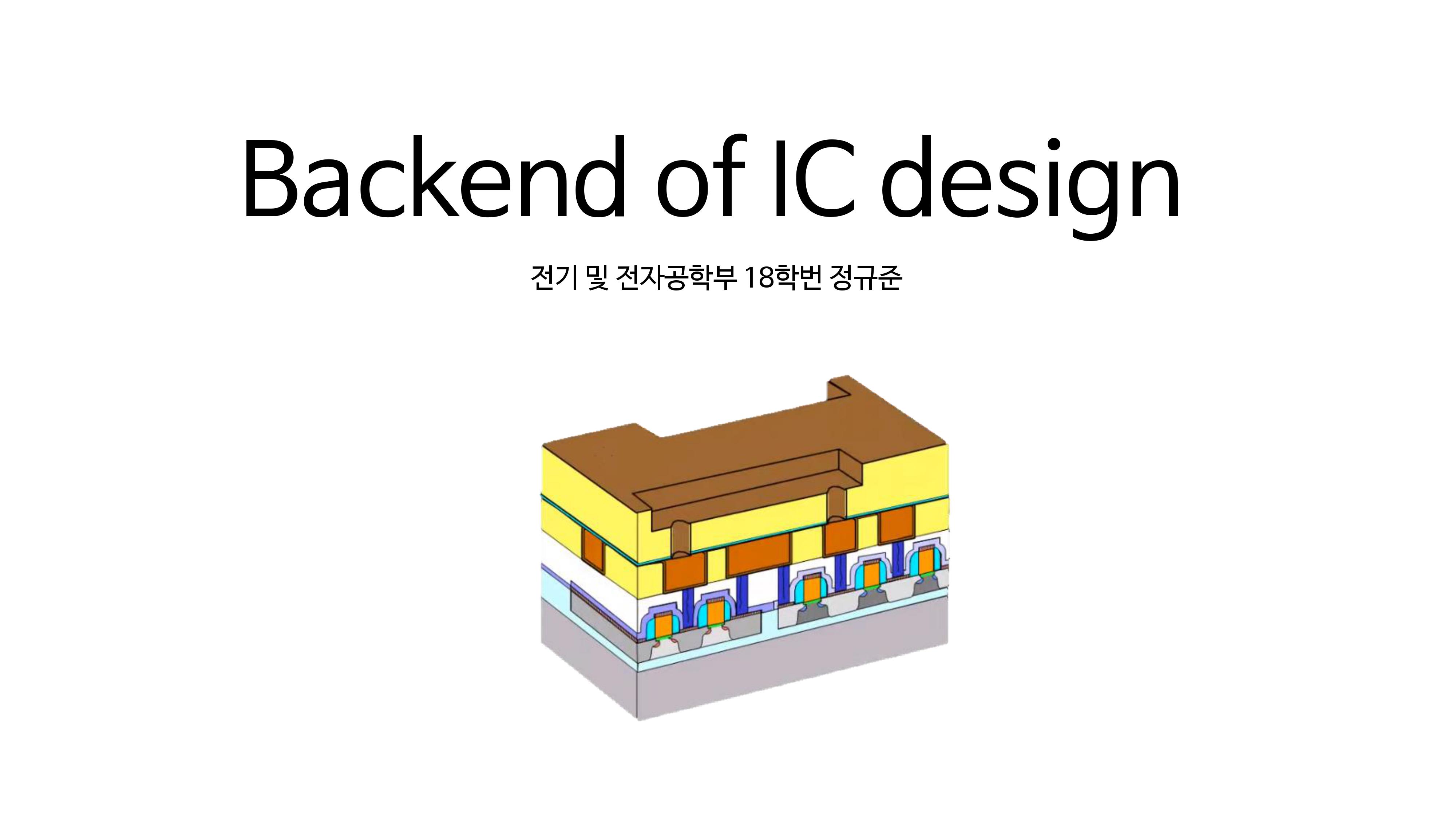
 Semiconductors were manufactured through the semiconductor process introduced in the previous posting. However, semiconductors that are simply lumps of silicon do not perform their functions. Today, let’s look at the backend design, which is a subsequent process.
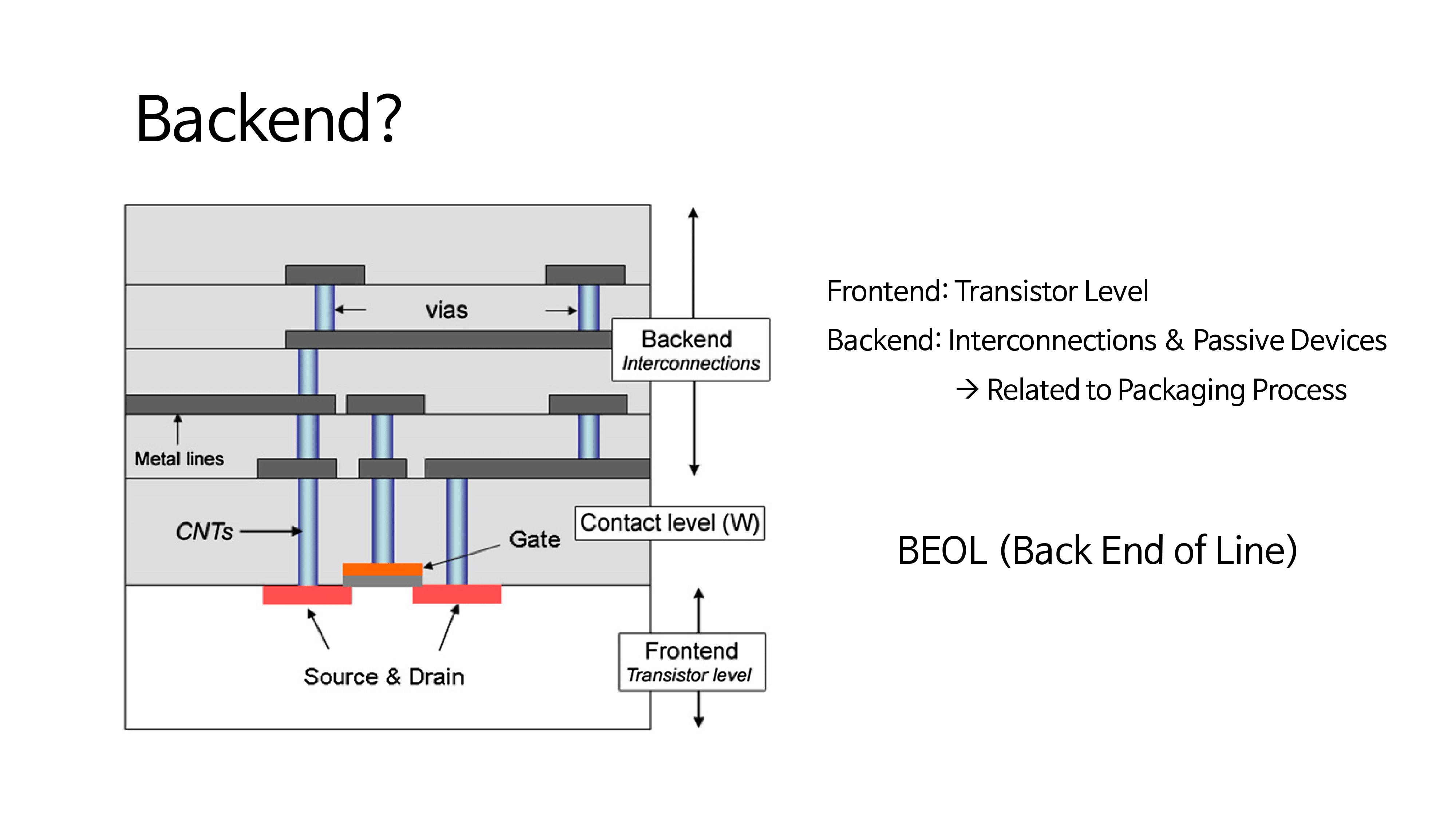 A frontend is a process at the Transistor level as in the previous posting method. A backend is a process of making chips with passive devices such as Interconnection or L or C.
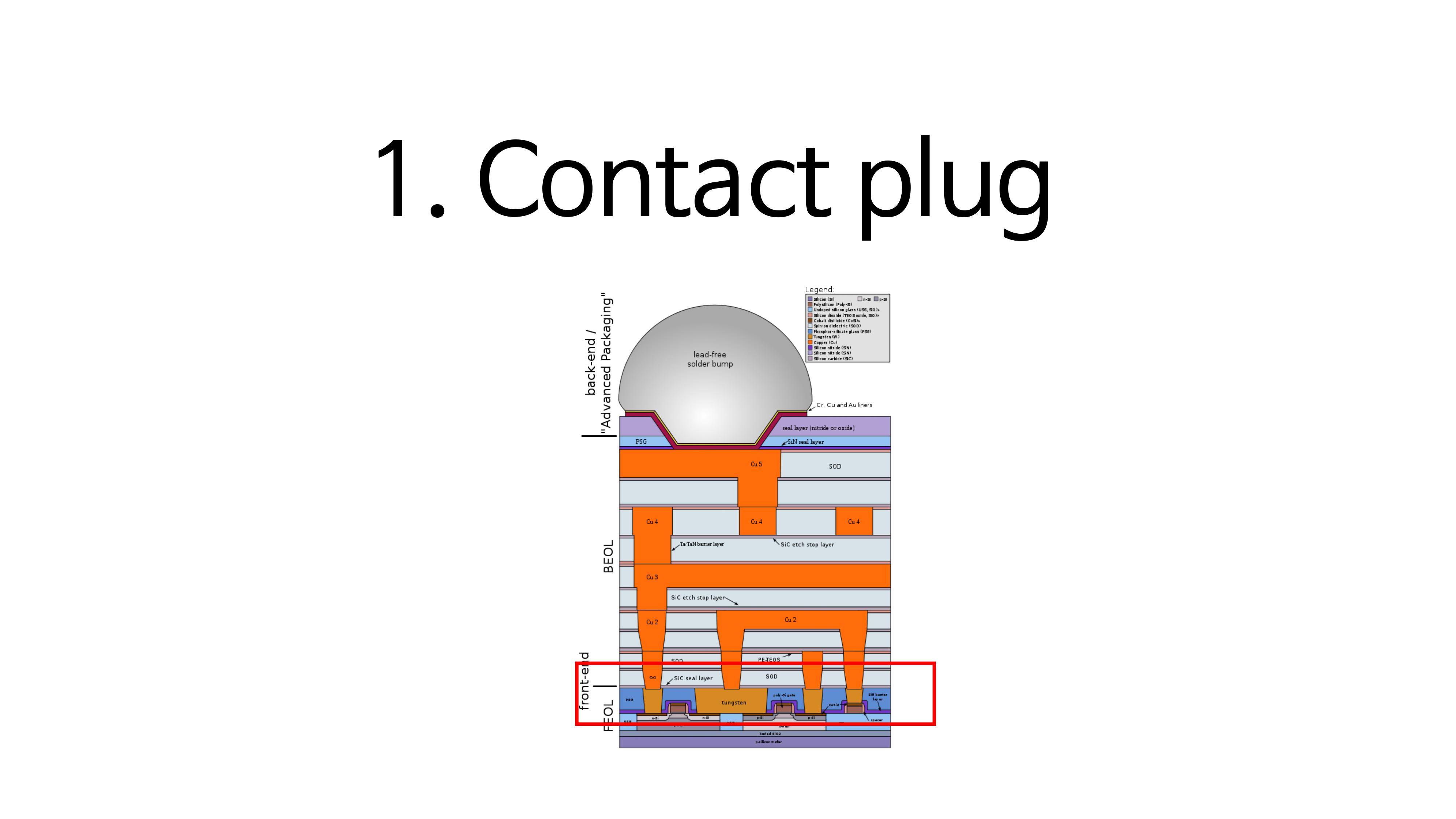 First, we must contact the plug that will act as the electrode of the designed transistor. Let’s take a closer look at this process.
 First, cut the thick oxide layer through etching.
 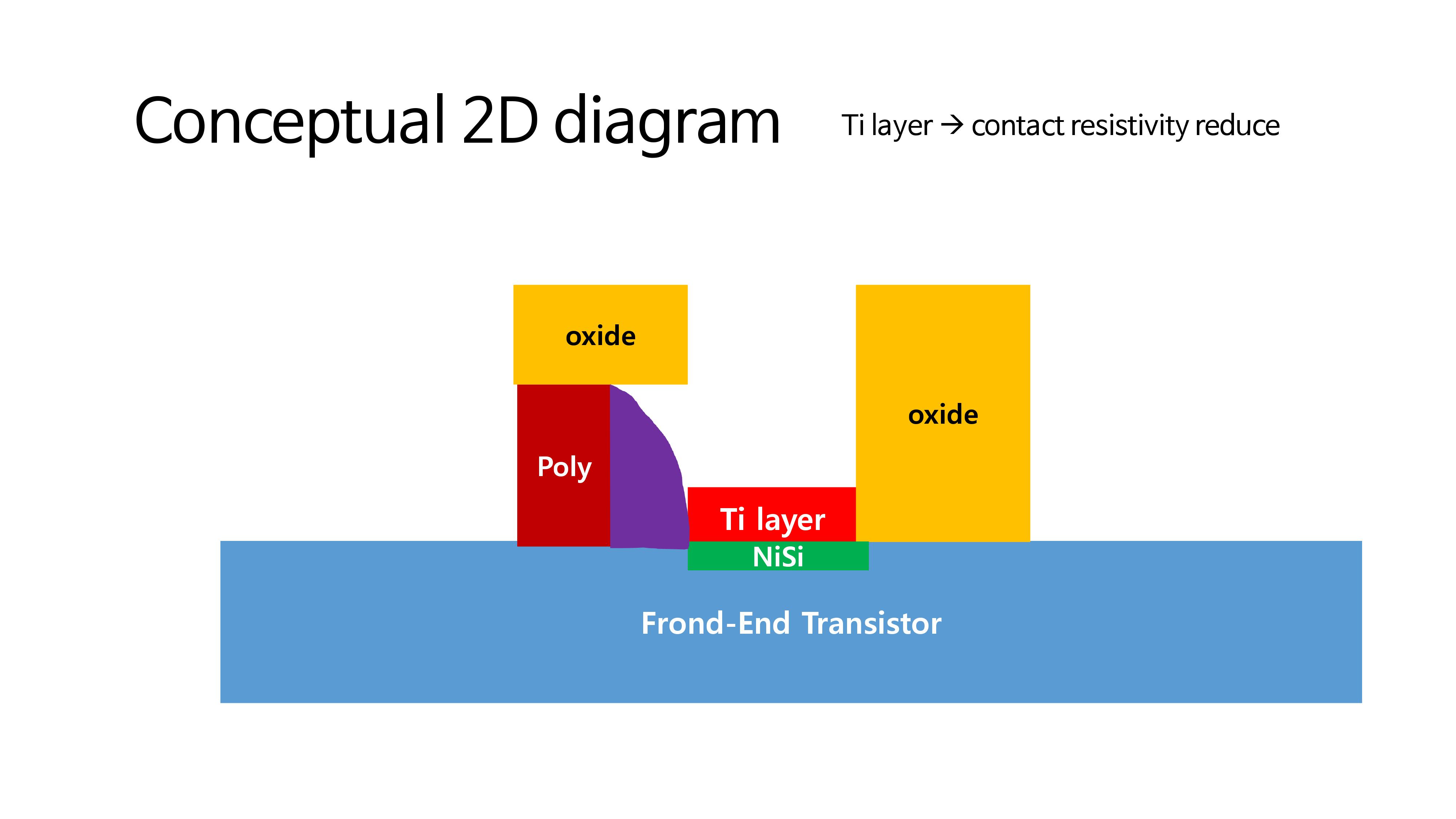 Then, cover the titanium layer with low contact resistance.
 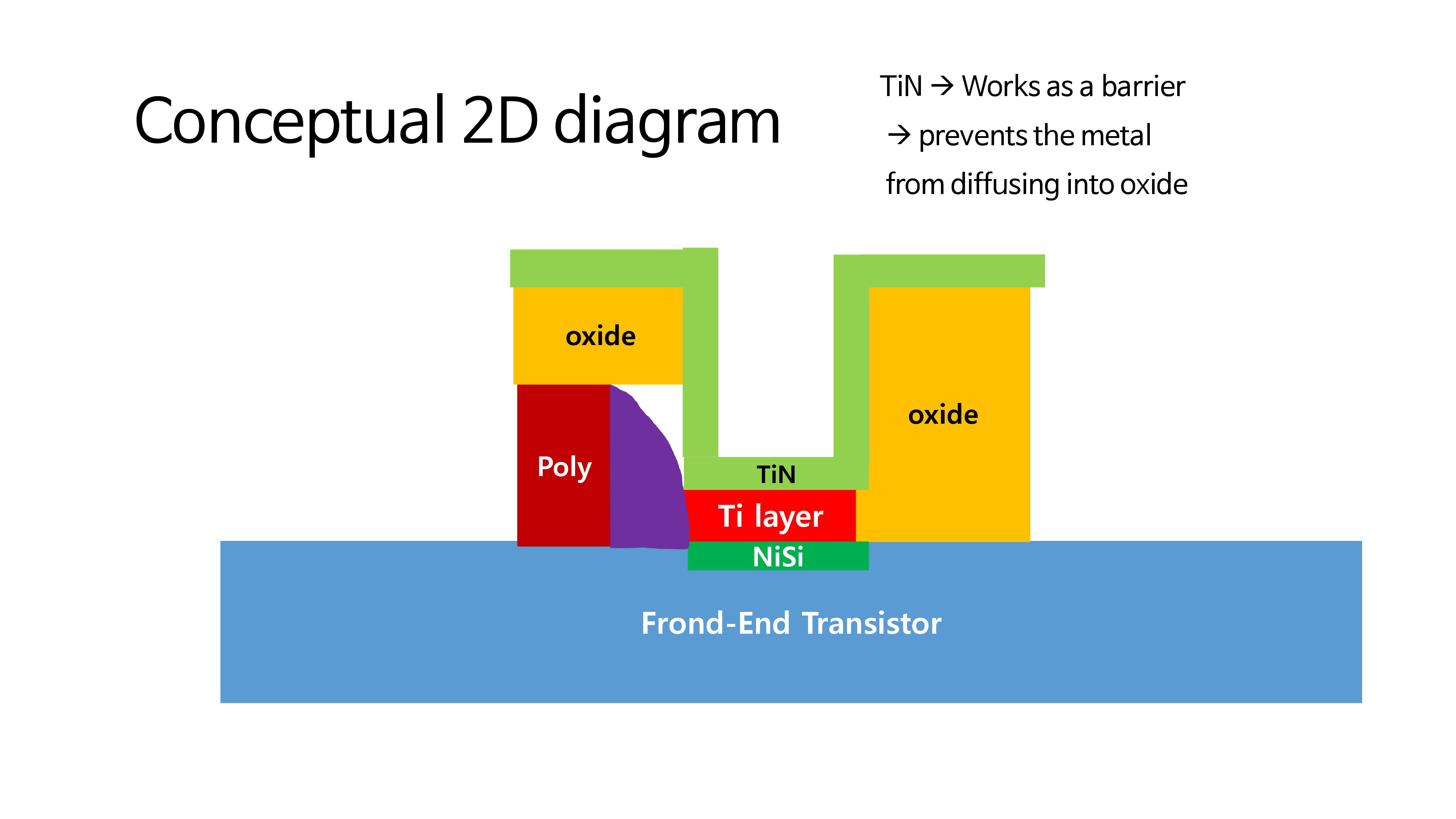 TiN acts as a barrier, preventing the metal to be pluggable from diffusing into oxide.
 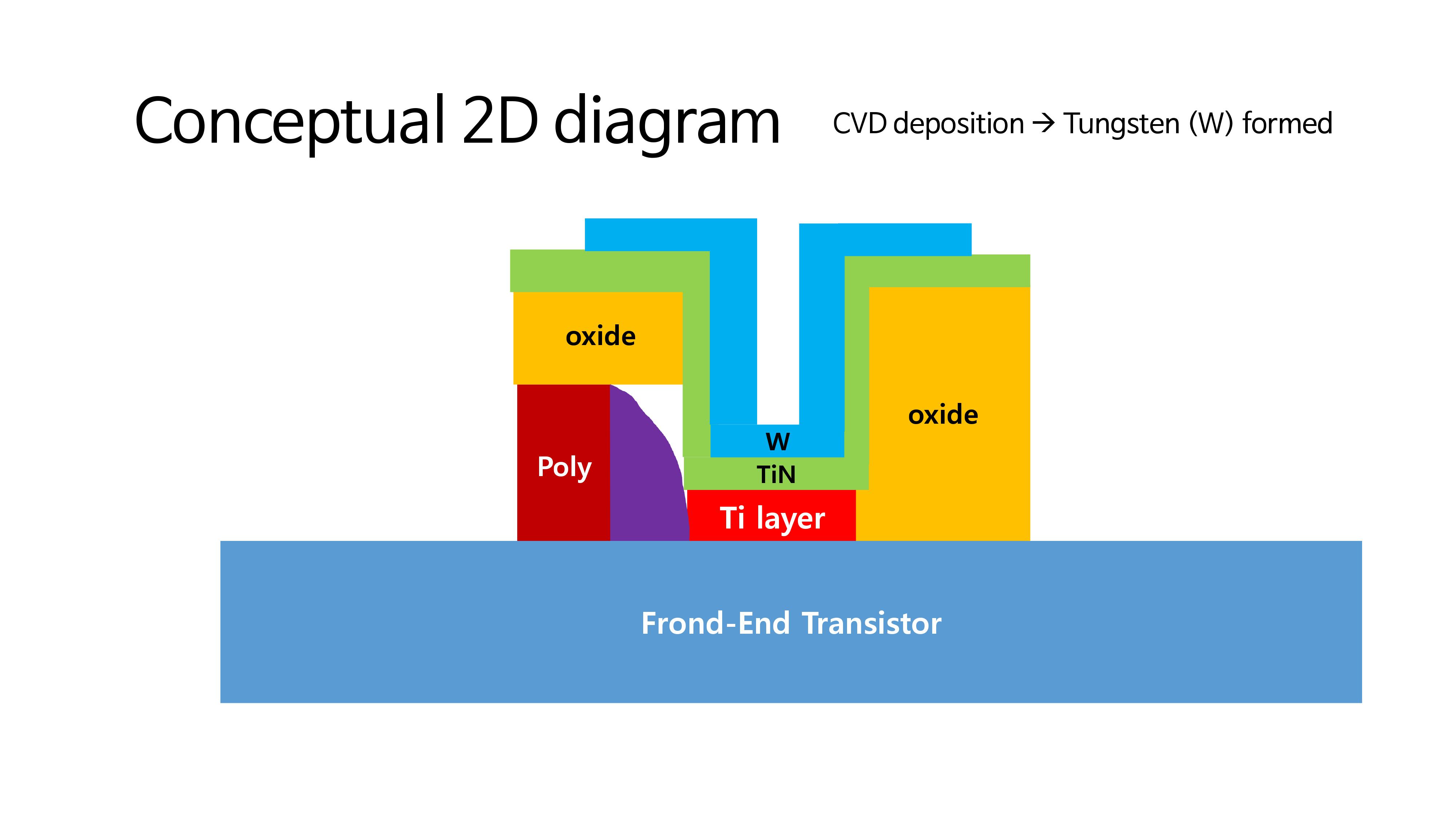 Thereafter, a tungsten (W) to serve as a plug is covered through a CVD deposition process.
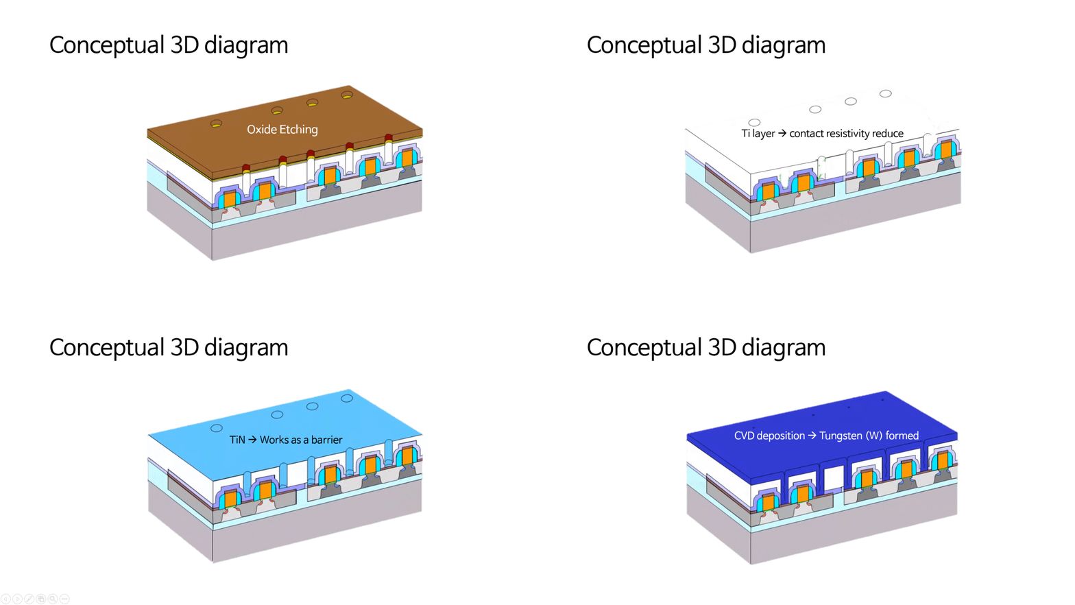
Continuous representation of this process results in the following. 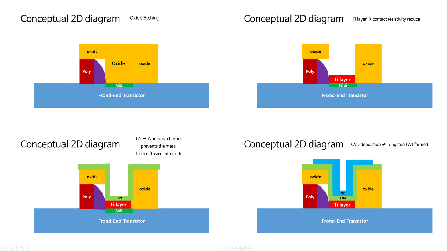 If this process is represented by 3D structure, it will be as follows.
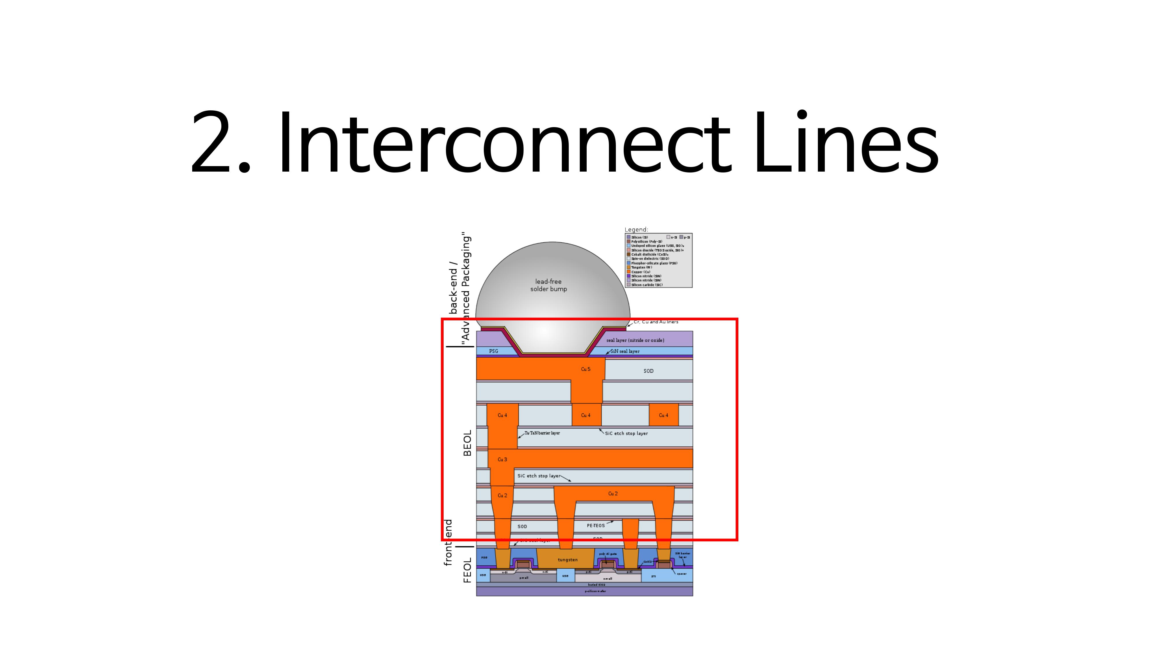 Since we installed the plug, let’s find out about the interconnection line that will connect these plugs organically.
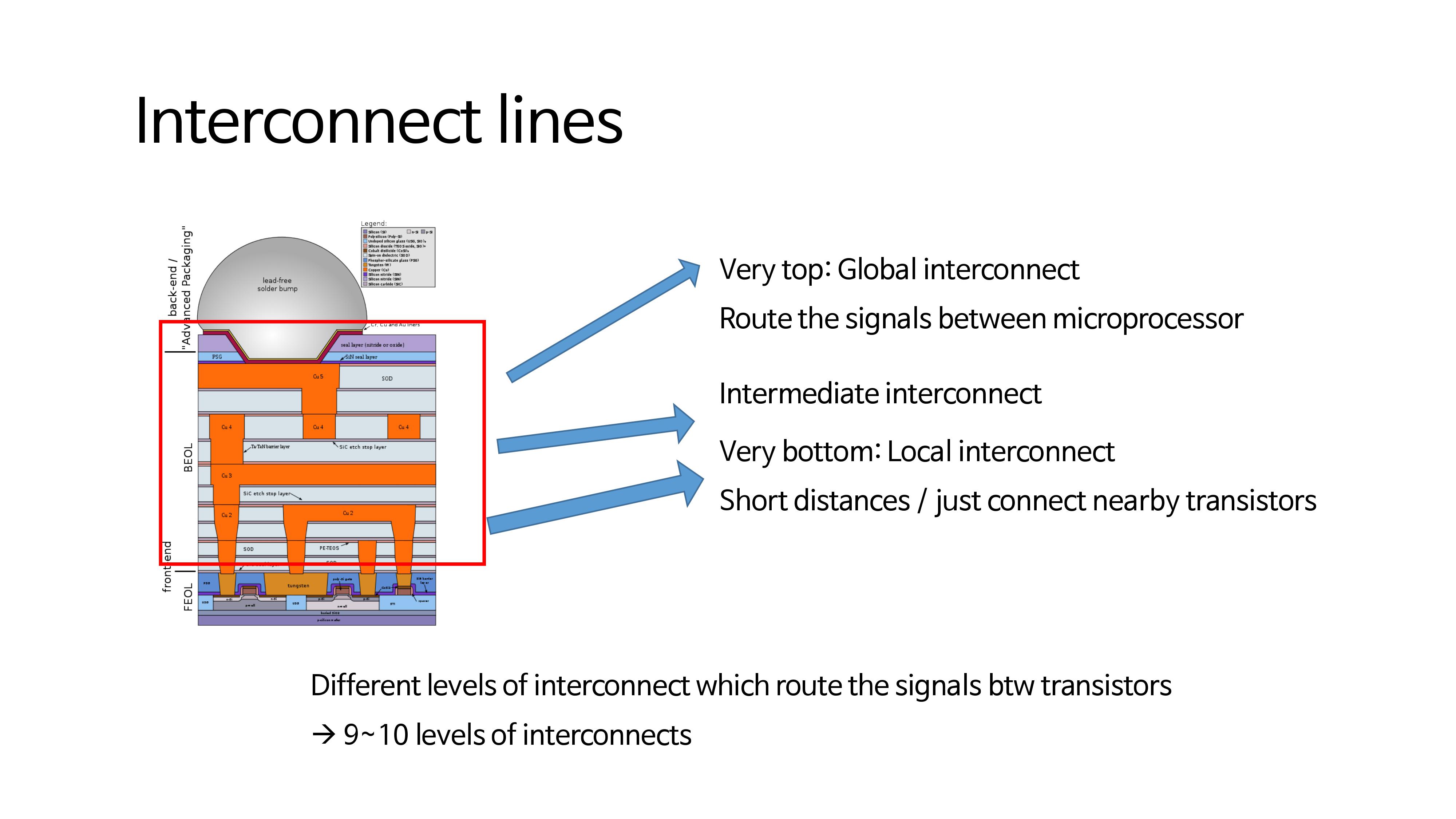 As shown in the figure above, the interconnect line layer can be stacked upward on 9-10 layers or more, and serves as a channel for exchanging signals between transistors.
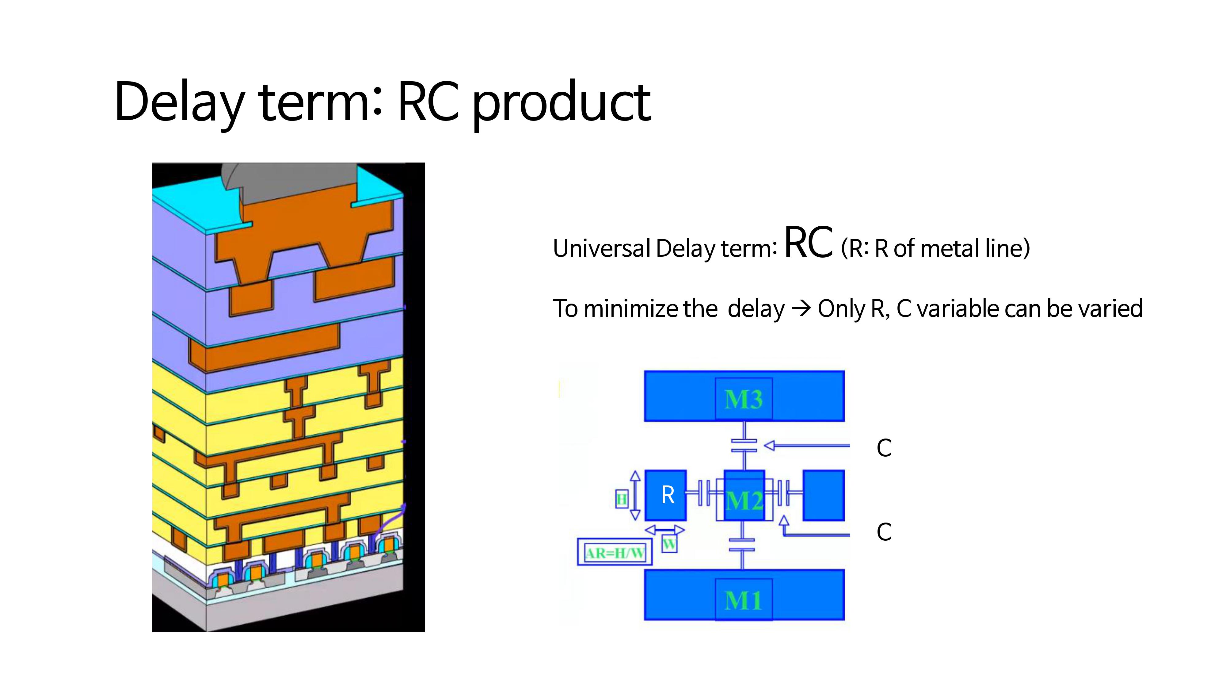 The most important term in this integrated circuit is RC product, which increases the delay. Delay can be minimized by adjusting R and C.
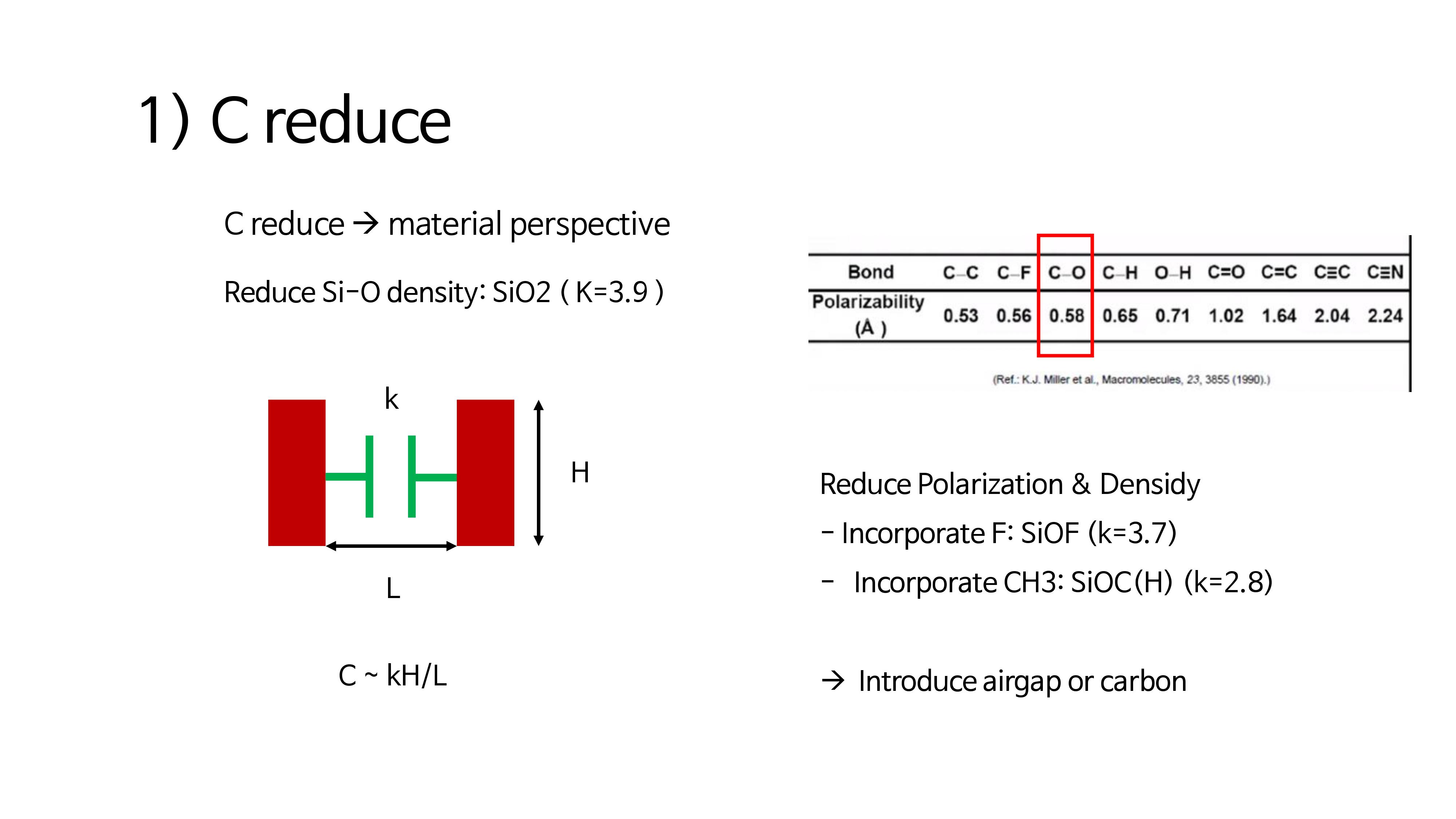 First, how do we reduce the Capacity(C)? From a material mechanical point of view, the dielectric constant of SiO2 in general is 3.9e. Looking at SiOC reduces polarization, which reduces K. This allows the reduce of C. In another way, it is possible to reduce C by introducing Airgap.
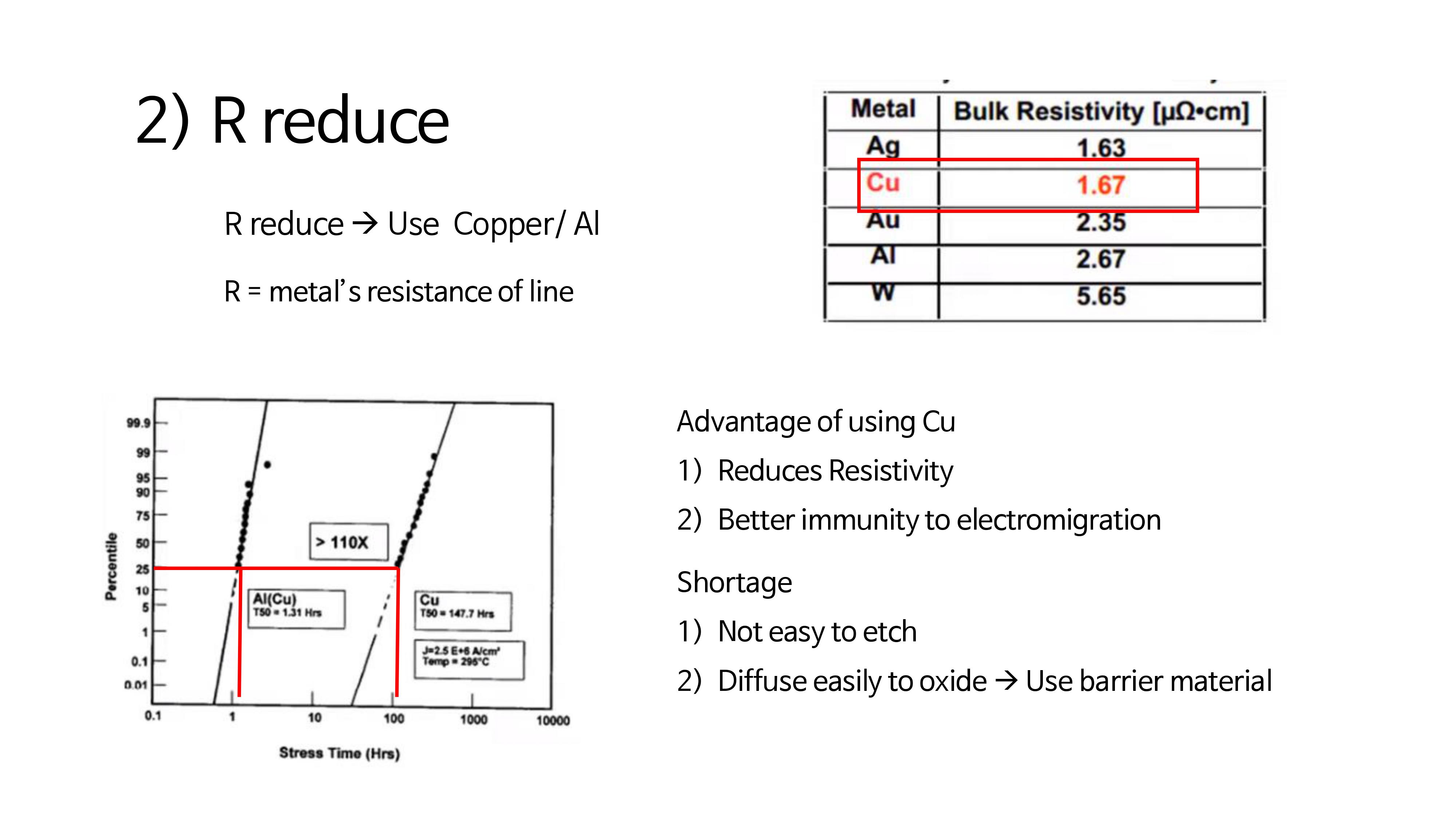 How can Resistance(R) can be reduced? You can use Cu or Al with the same resistance. Let’s take a look at the bottom information below.
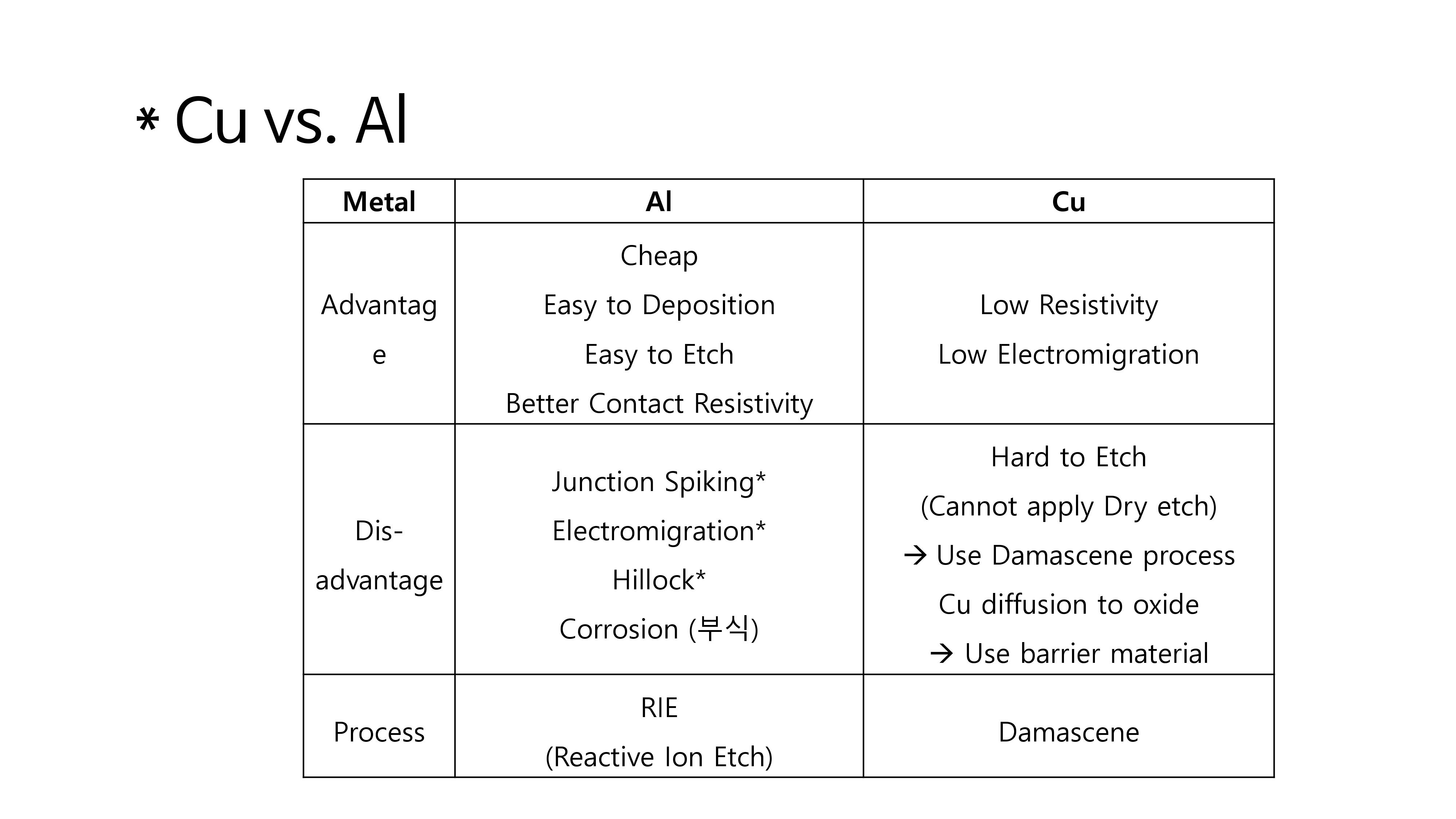 Since Al and Cu have different physical properties as described above, the metal wiring process of the two is completely different. The wiring process of aluminum is called RIE, and the wiring process of copper is called Damascene process. The term asterisked here may be unfamiliar, so let’s find out.
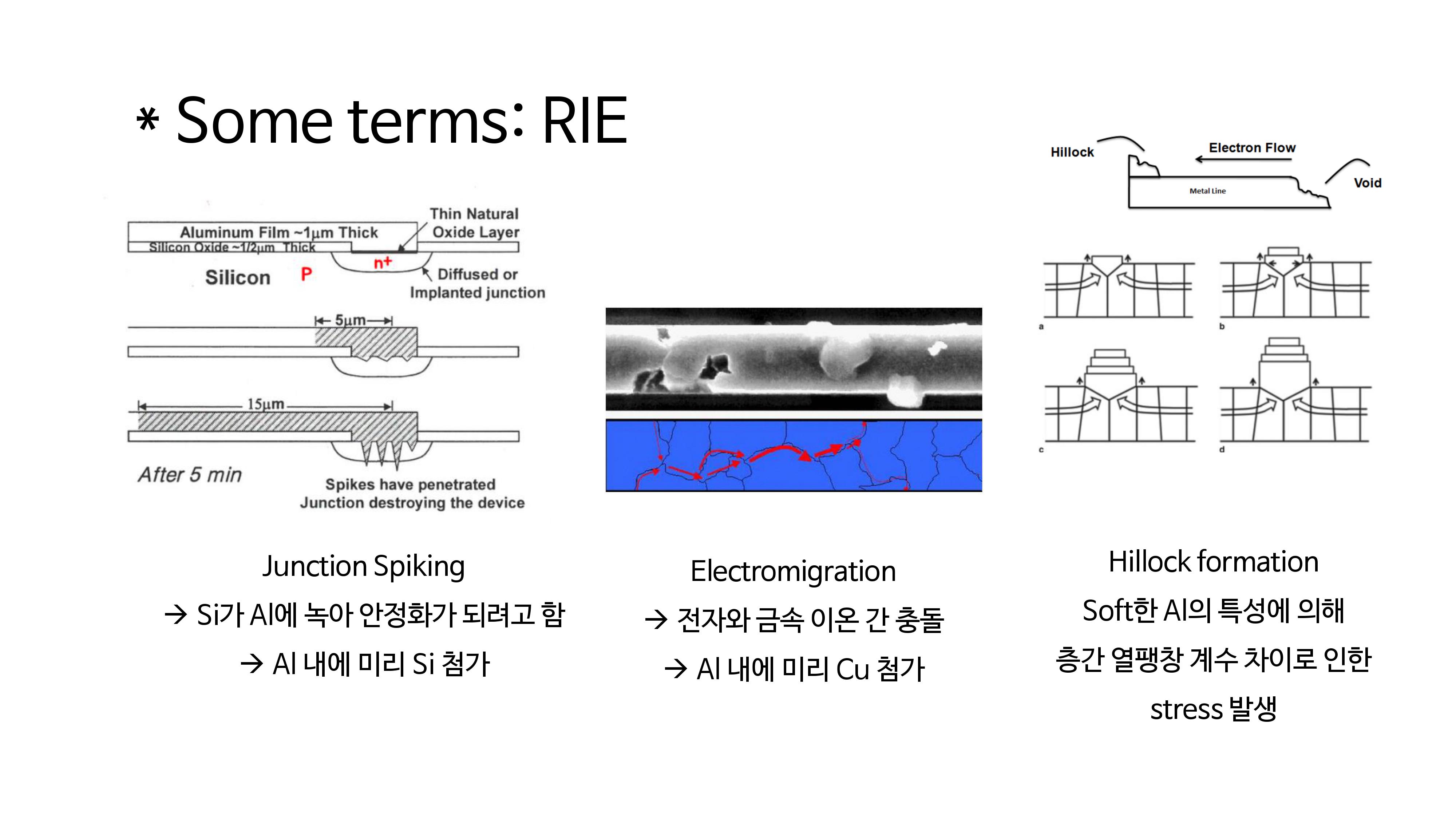 I summarized the terms above. Moving on to the main point, let’s find out the difference between RIE and Damascene processes.
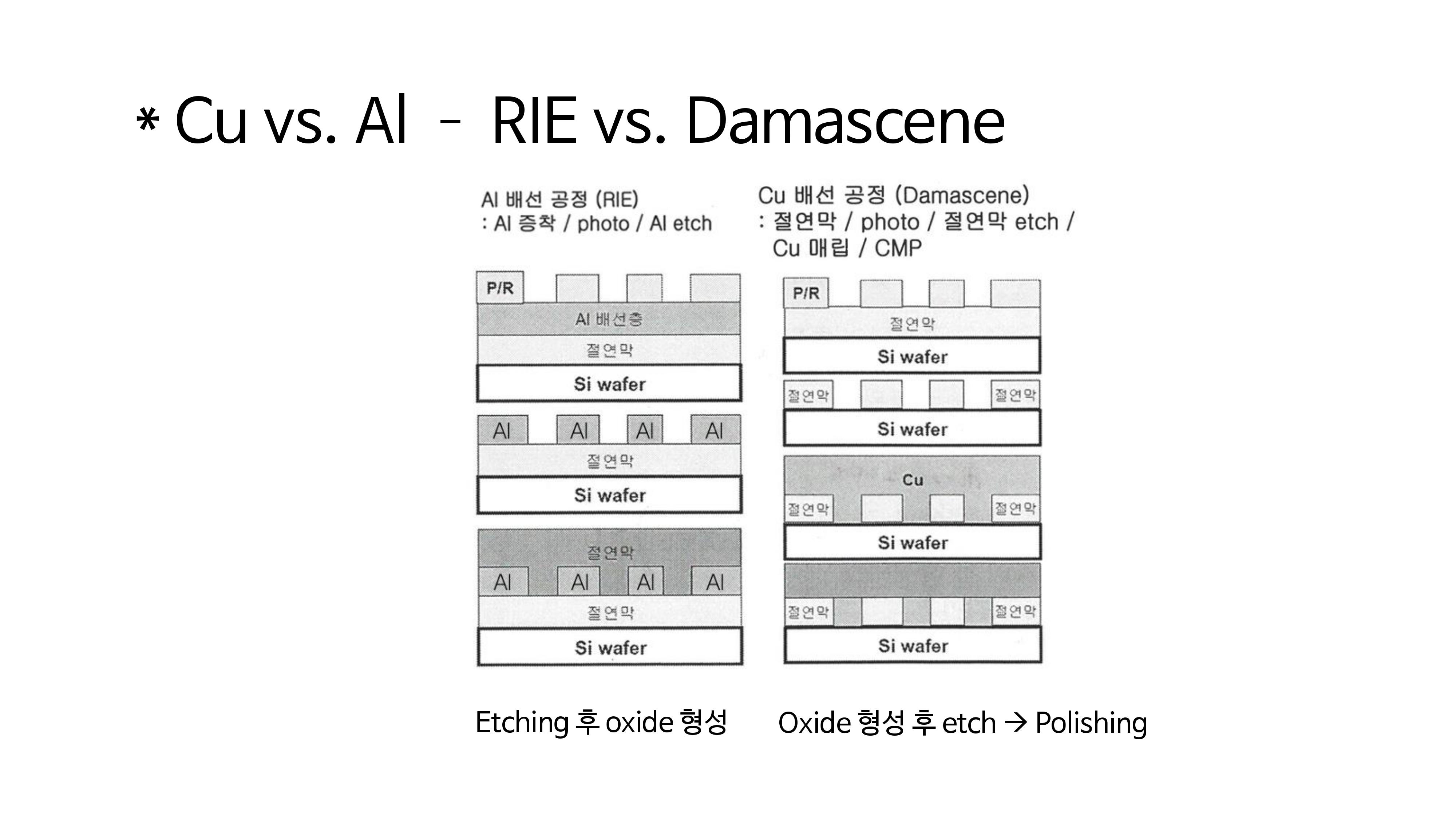 The key difference between the two processes is in order. The RIE process forms oxide after etching, and since the Damascene process is difficult to etch as shown in the above table, there is a sequence of forming oxide, etching, and polishing the protruding part. It’s easy to think that the two are in the opposite order.
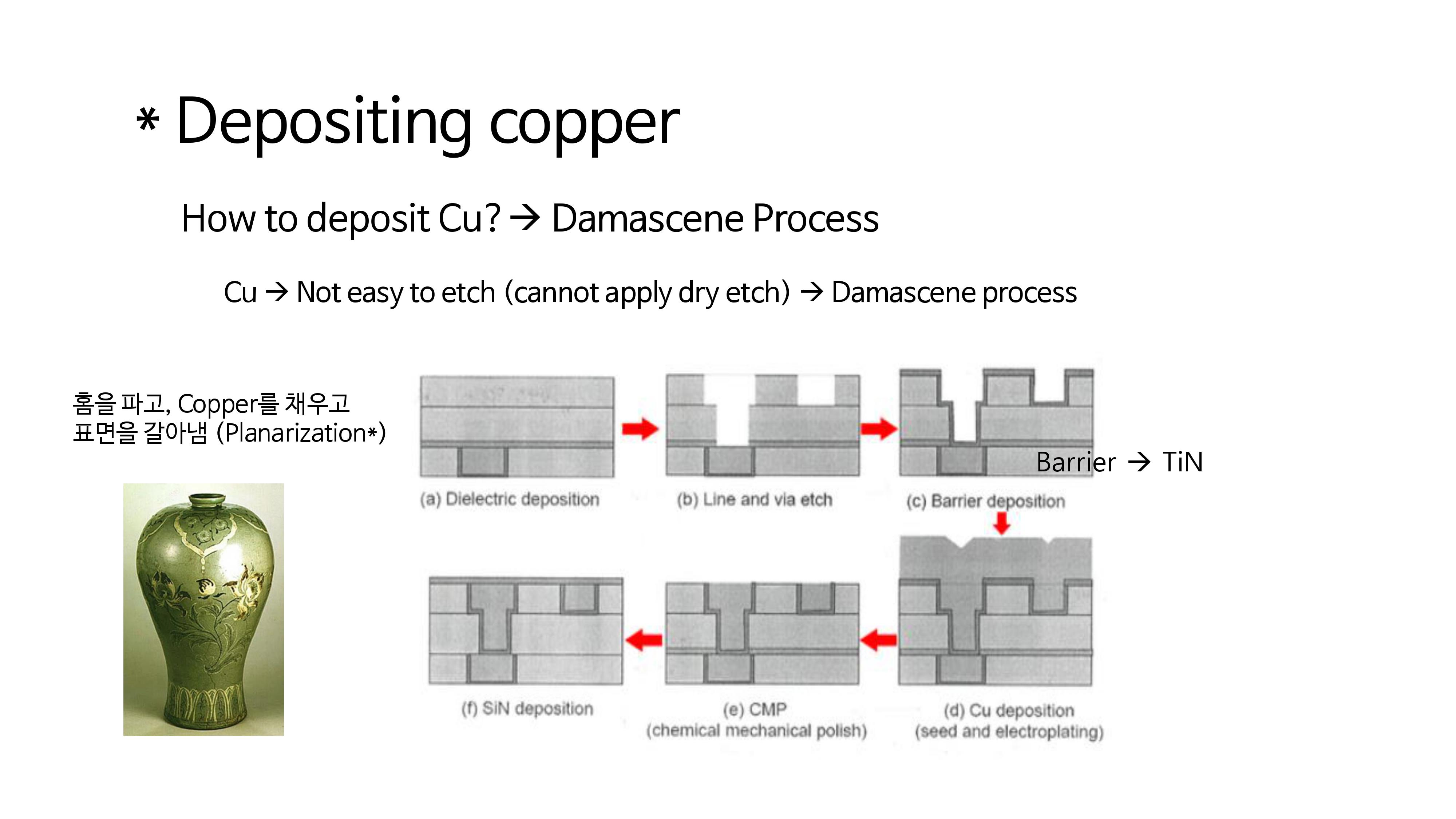 Let’s find out more about how to deposit the Copper. The Damascene process can be considered as an inlaid technique, and when making pottery, it uses a technique of digging grooves first, filling with other materials, baking, and grinding the surface, which also has the same process.
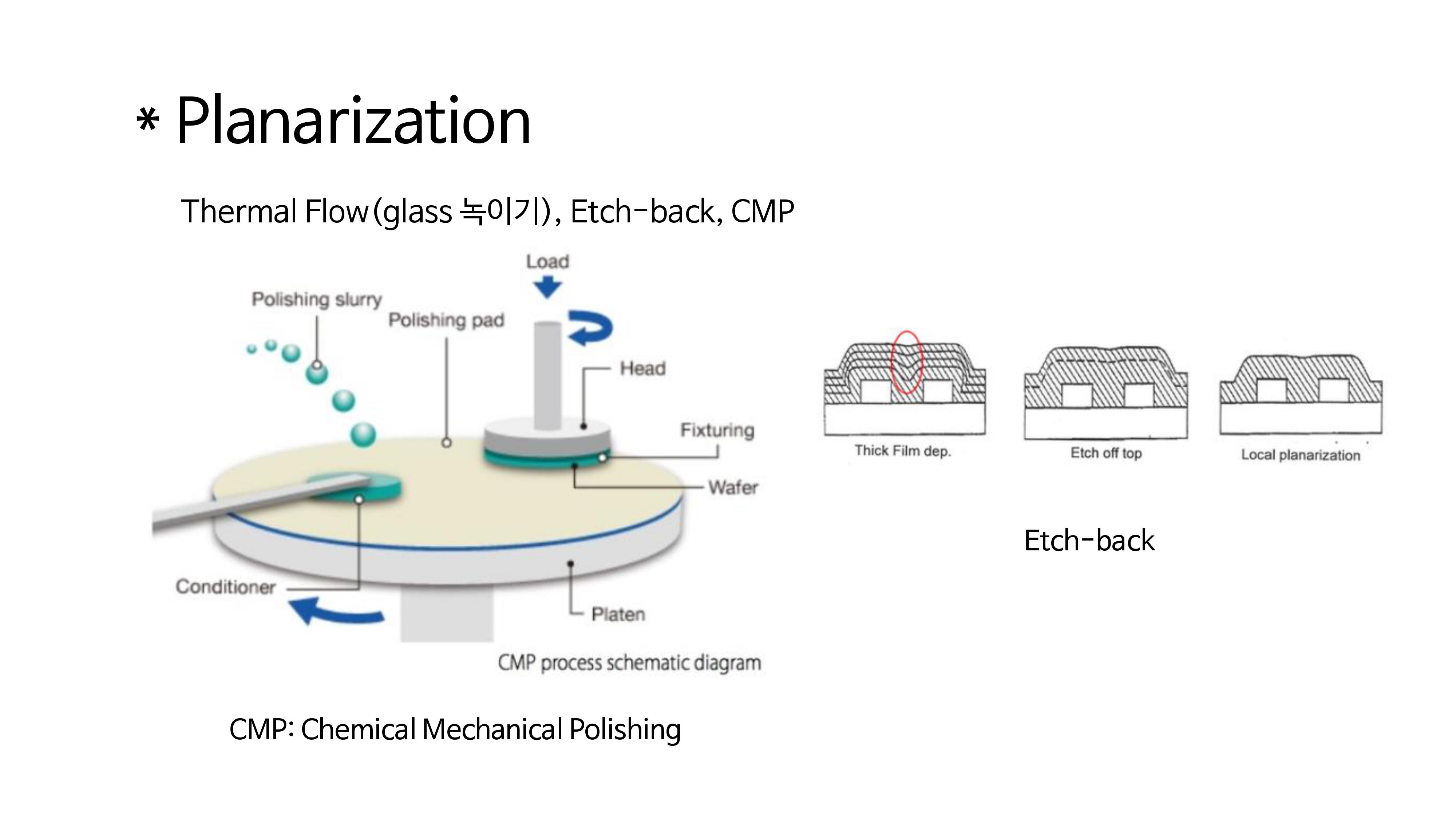 The surface grinding technique is called the planarization process, and the surface can be polished through various processes such as Thremal Flow, Etch back, and CMP.
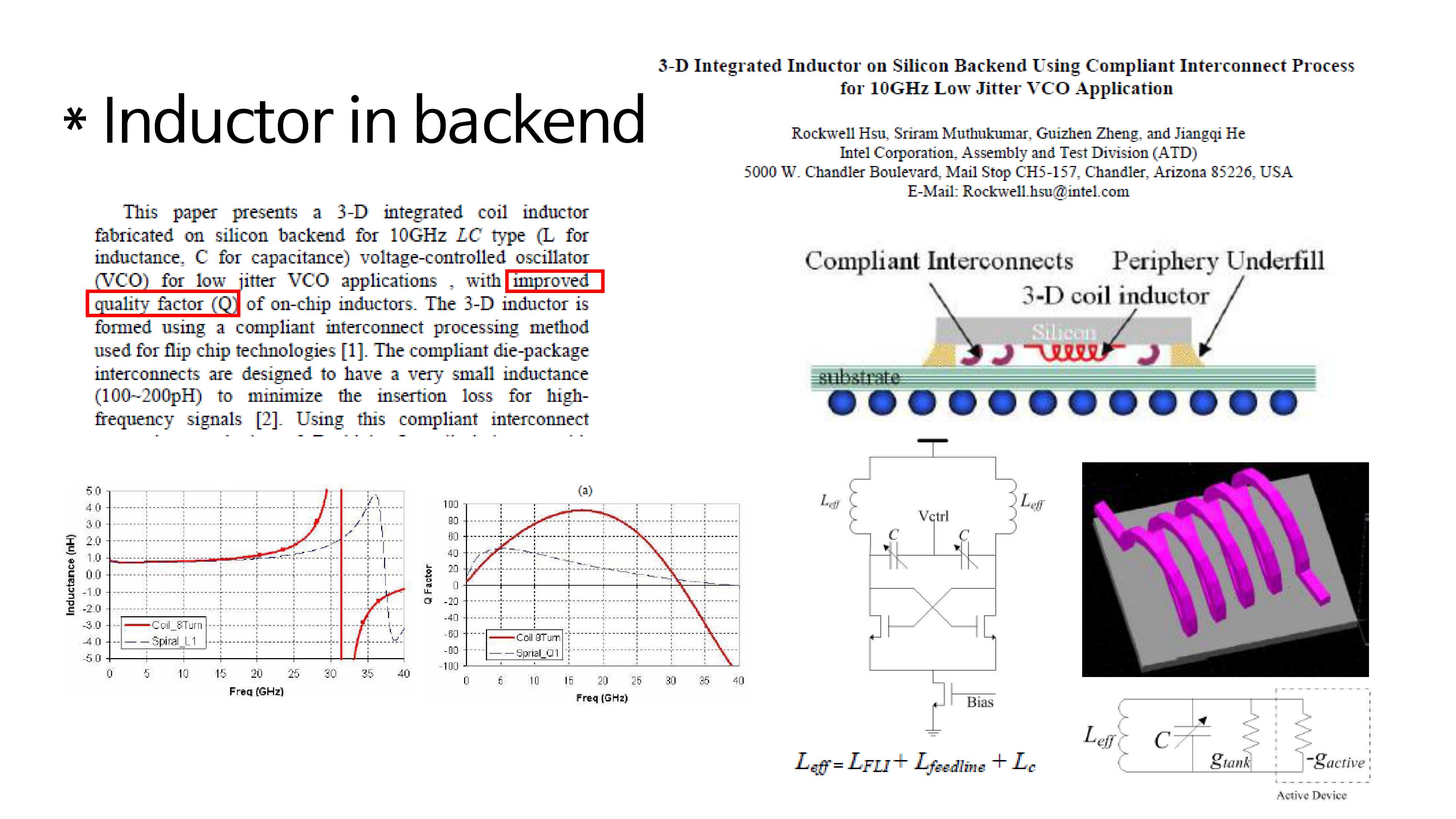 Among R, L, and C of passive devices, there has been no mention of L so far, so let’s briefly learn how to use an inductor. Intel’s Zheng researchers have been extracting papers, which can improve the quality factor by using Inductor.
So far, the metalization process, i.e., metal wiring process has been investigated. Now, the remaining processes are the EDS process and the packaging process, and we’ll talk about this later, and let’s just briefly talk about it now.
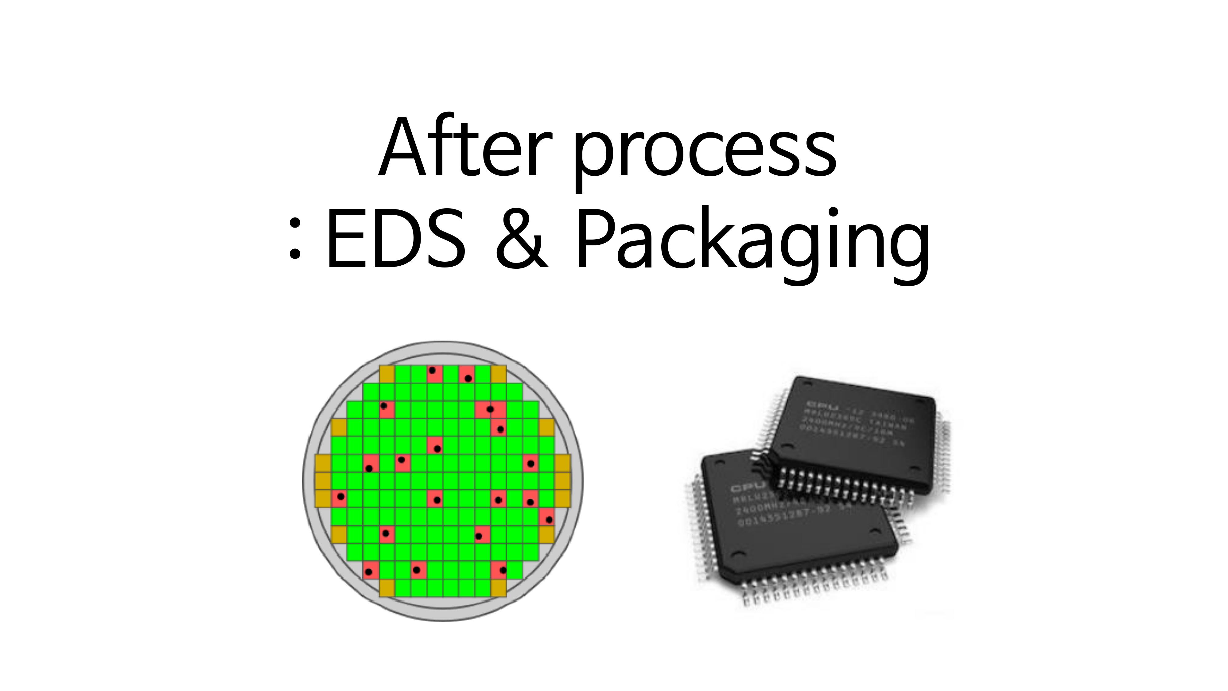
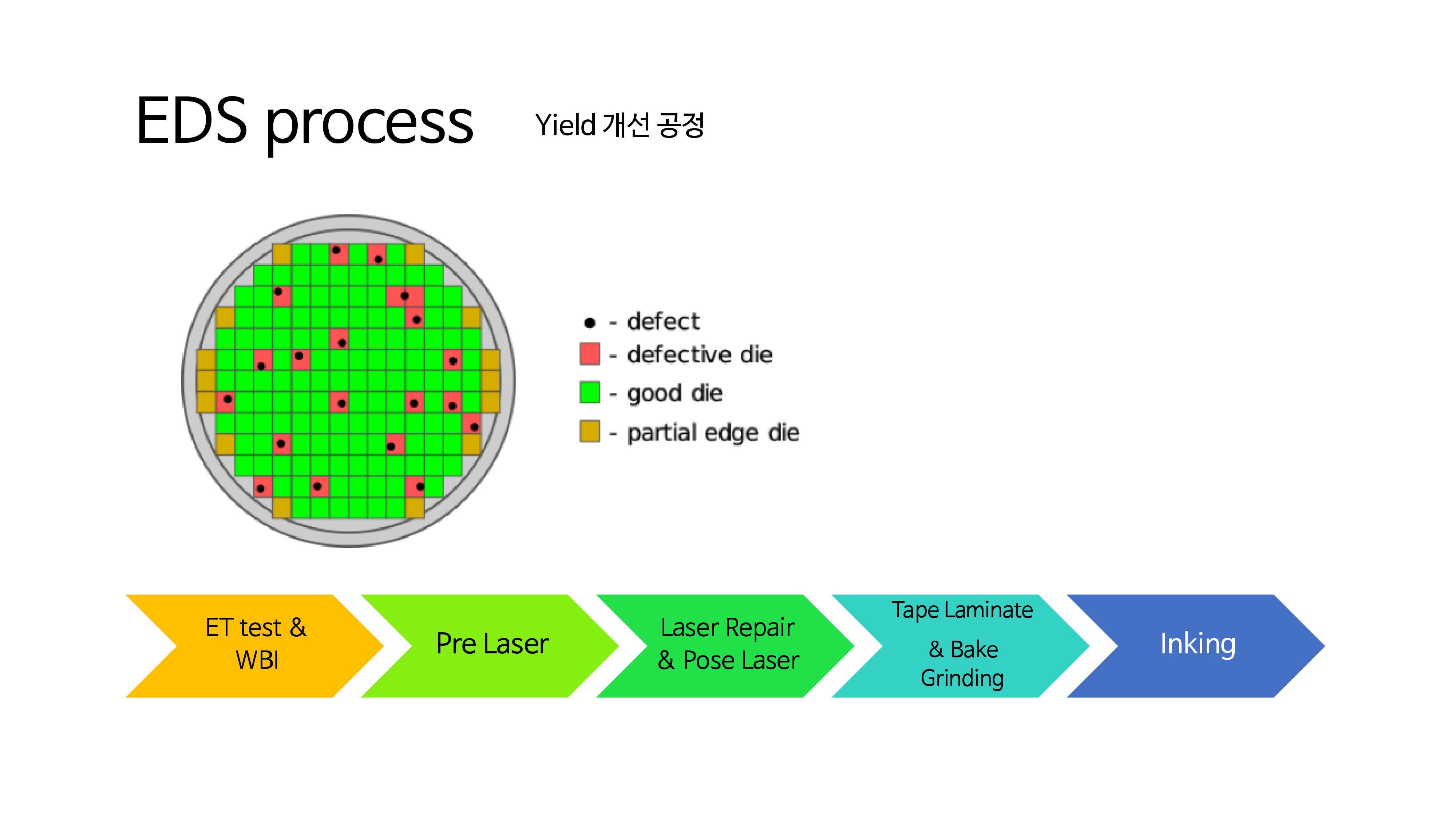
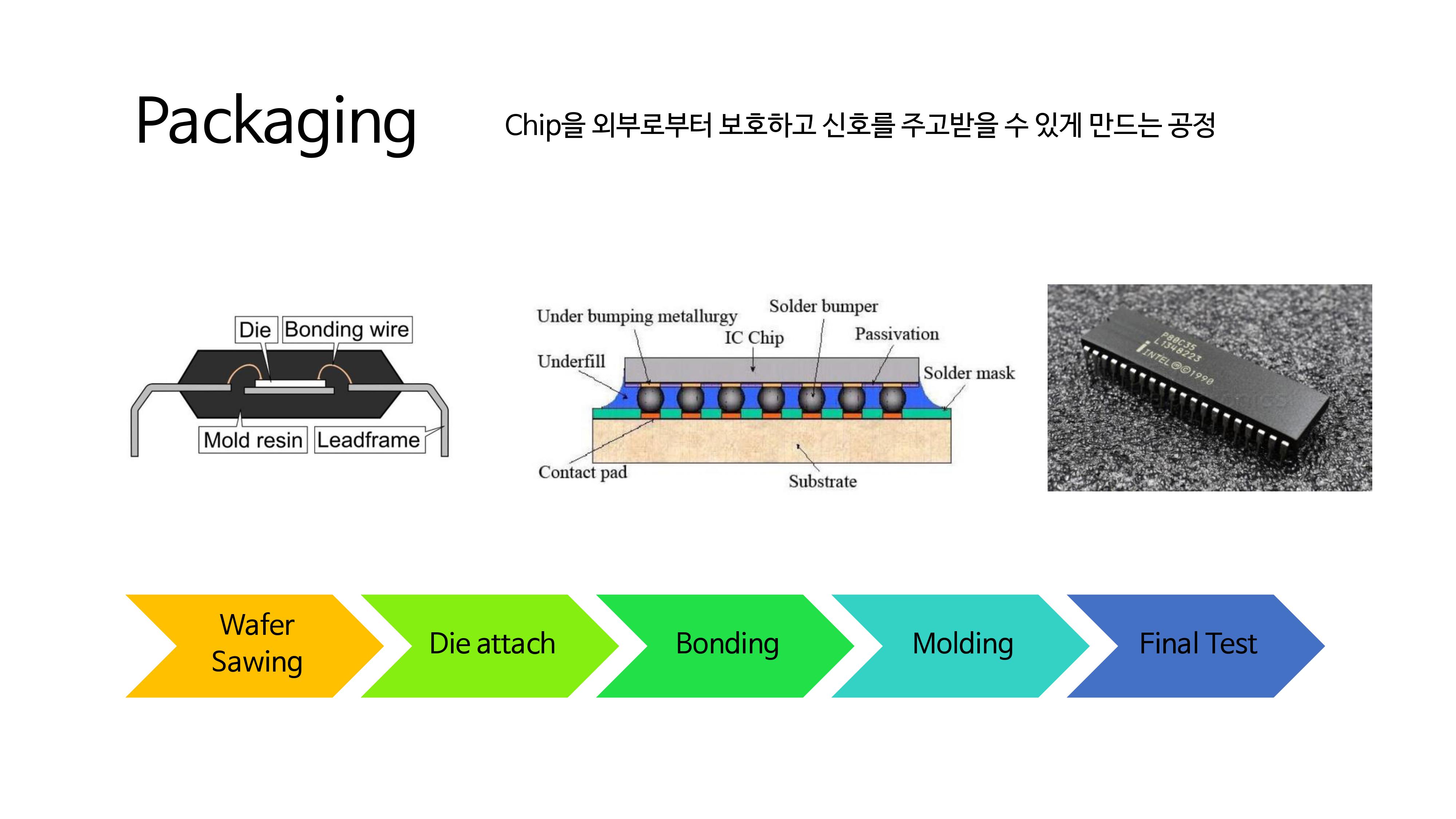
The EDS process is a yield improvement process, and the packaging process protects the chip from the outside and packages it so that signals can be exchanged. The detailed sequence can be found by looking at the picture above.
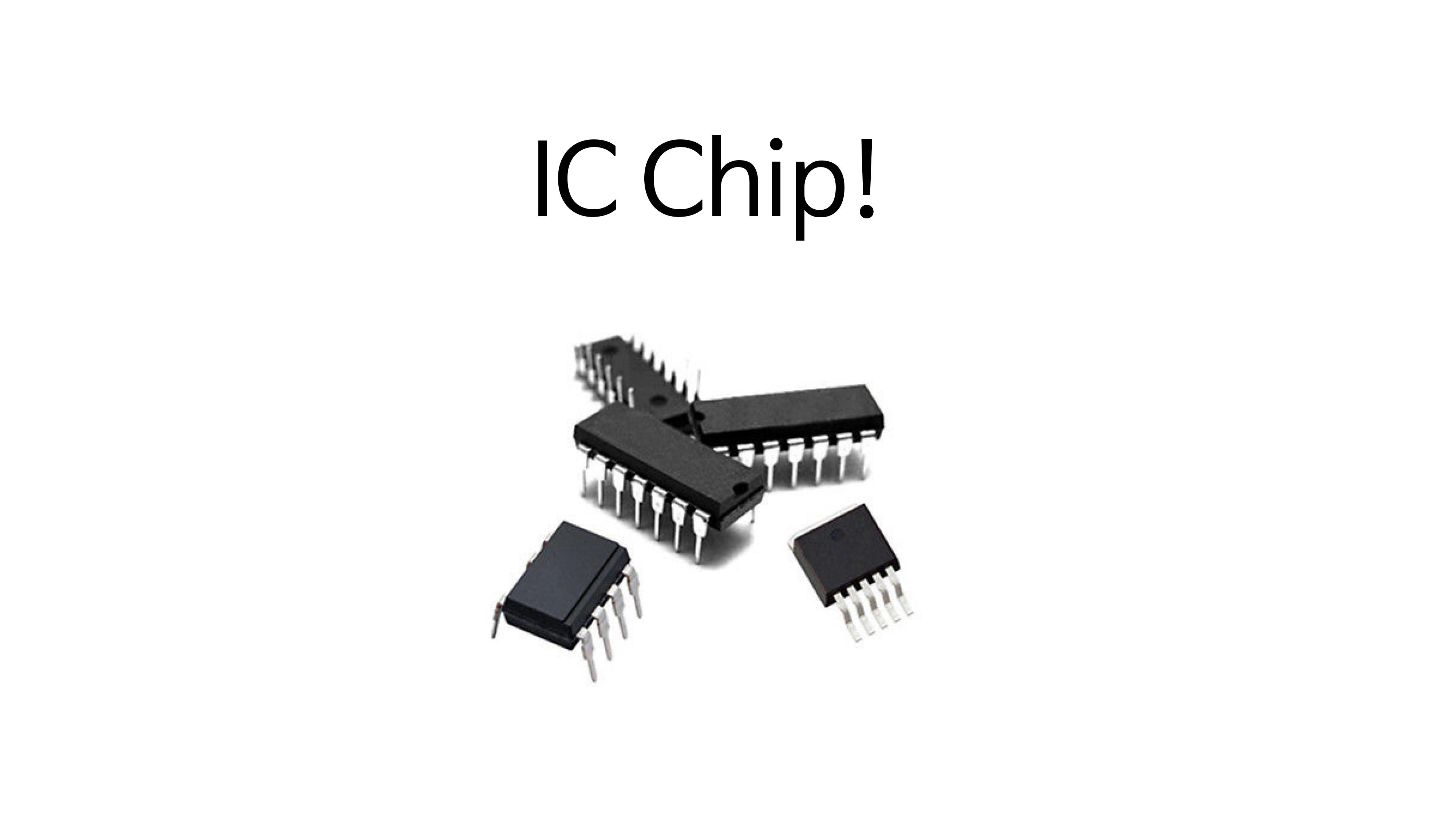 Through these complex and diverse processes, one IC Chip can finally be produced.