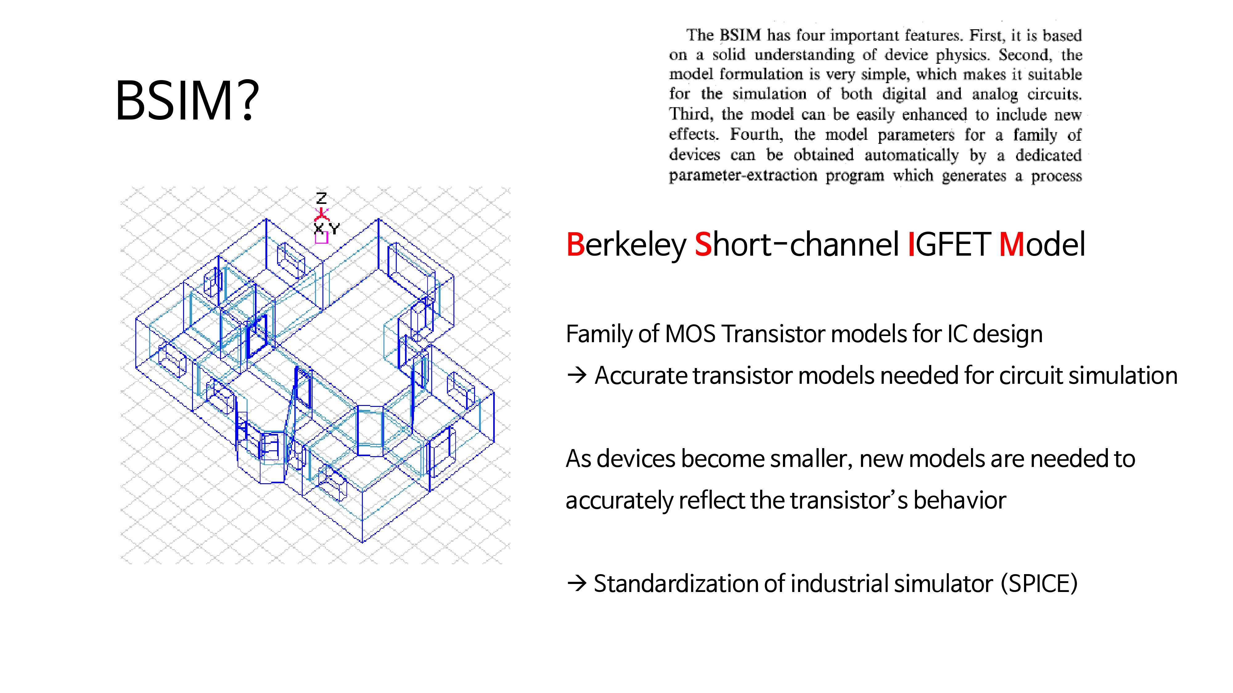
 Computer simulation is necessary to make MOS devices. There should be a model required for these simulations. As the device became smaller, a new model was needed to reflect the behavior of the transistor. A model performing this role was produced by UC Berkeley. BSIM is an abbreviation for the Berkeley Short-channel IGFET (formerly known as MOSFET) model.
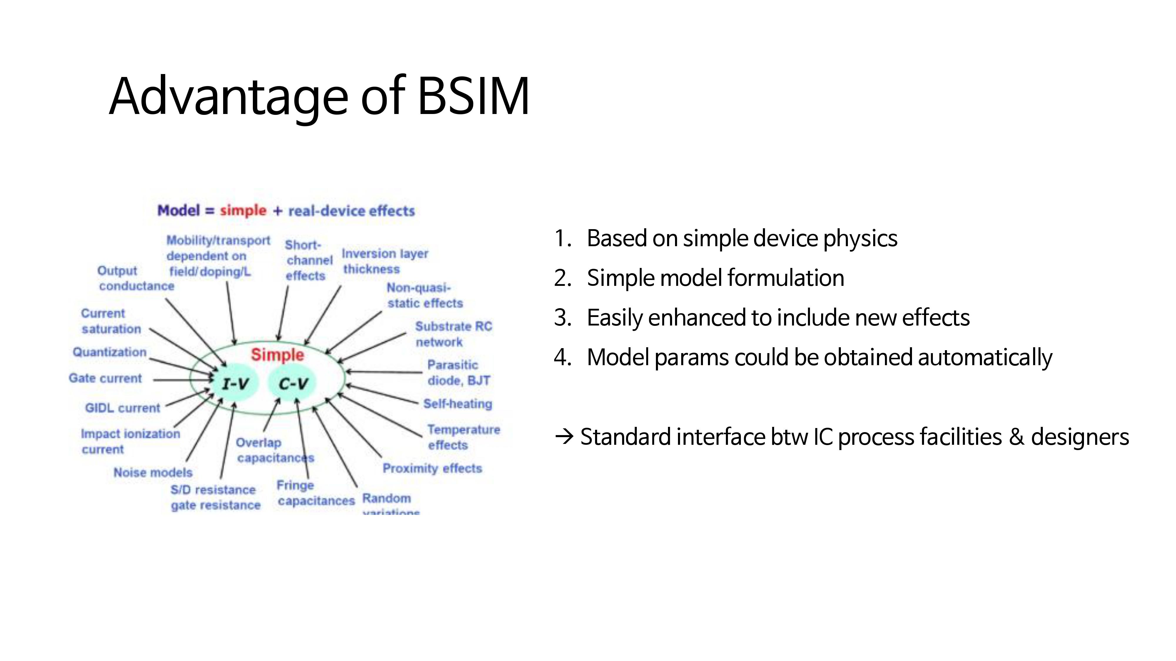 Let’s find out the benefits of using BSIM. BSIM is a model based on Simple Device Physics, which reflects physical phenomena well. It can also quickly reflect new phenomena, and all parameters are automatically calculated. With this advantage, BSIM is becoming a standard interface for designers and research institutes that design integrated circuits.
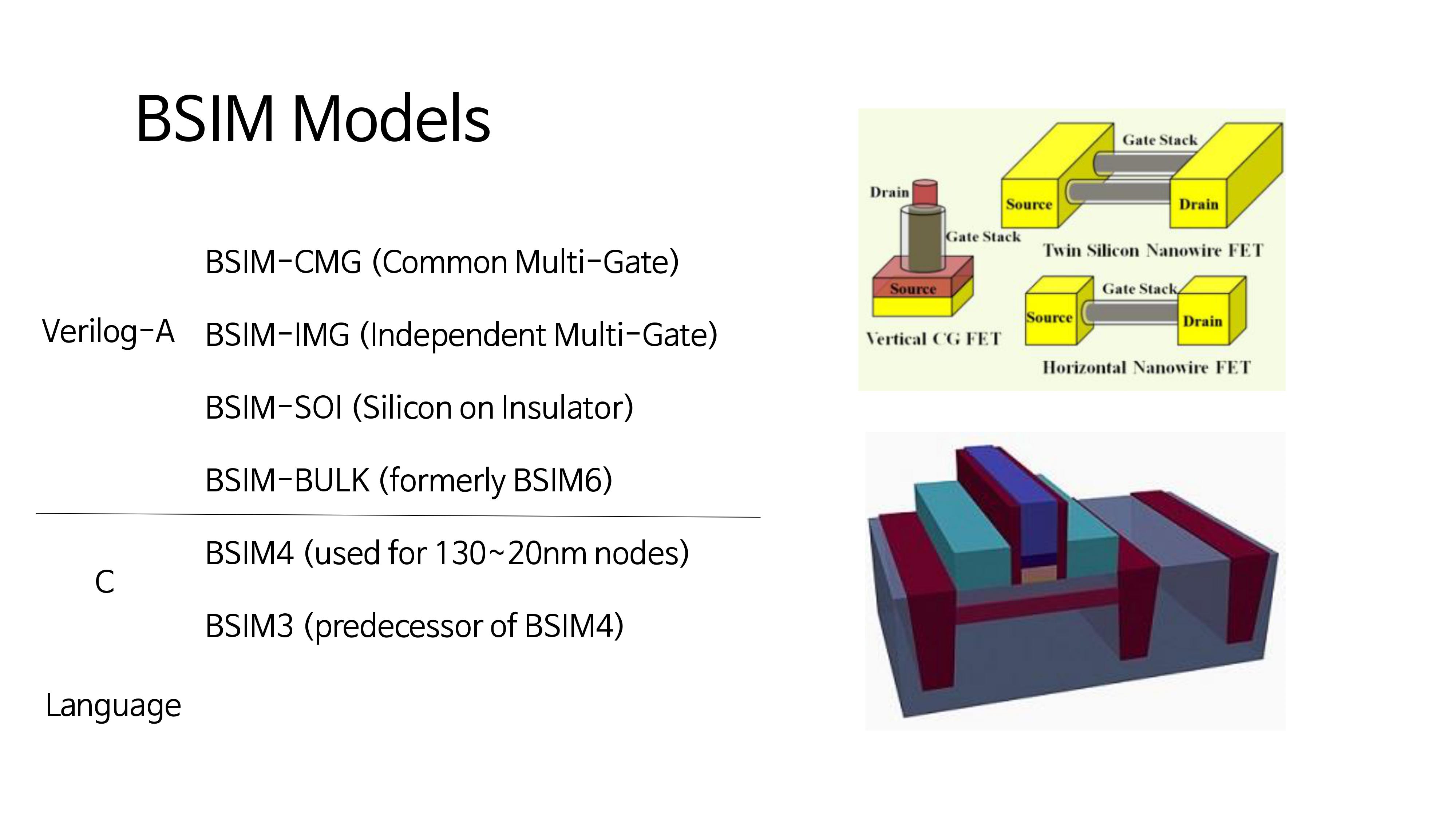 The BSIM model has been developed since the 1980s and has been in use until now. The model is older at the bottom, with the C language used up to BSIM4, and the Verilog-A used to model from later models.
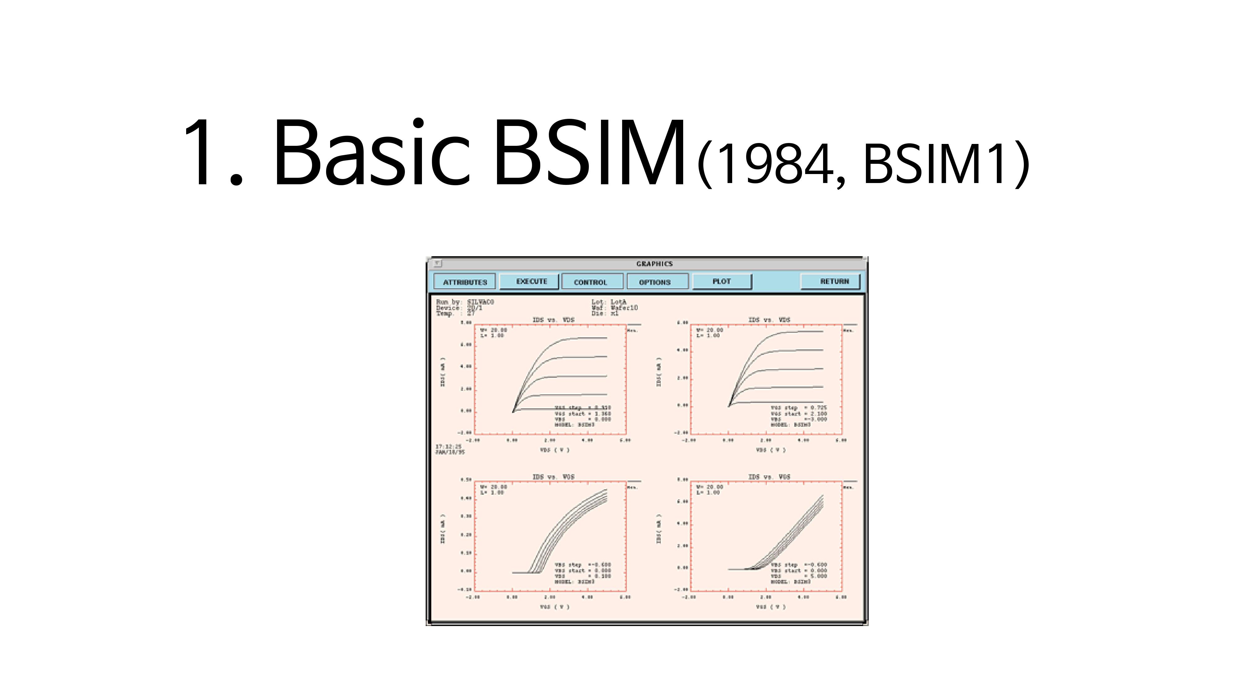 Let’s look at the basic BSIM model (BSIM1).
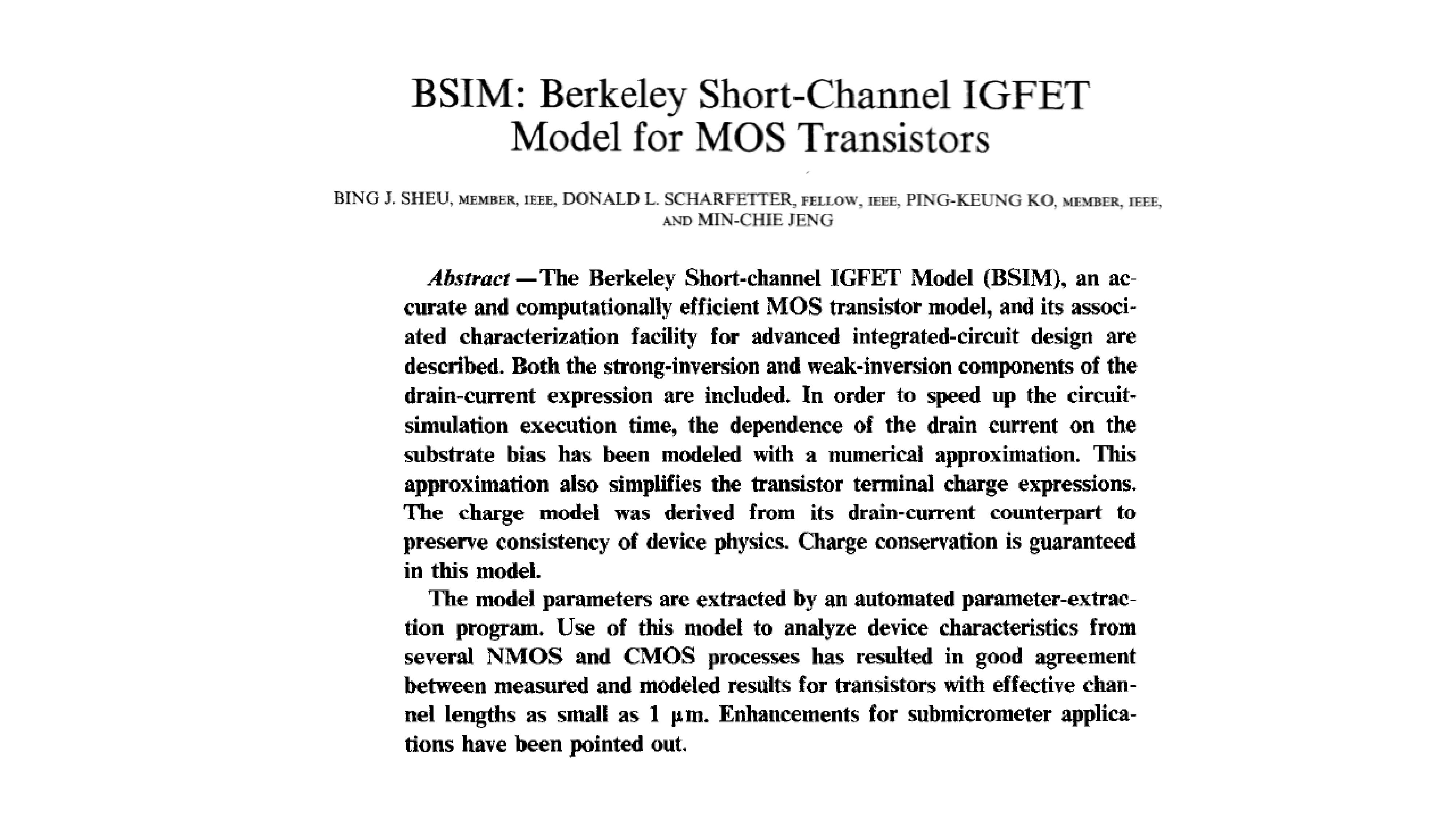
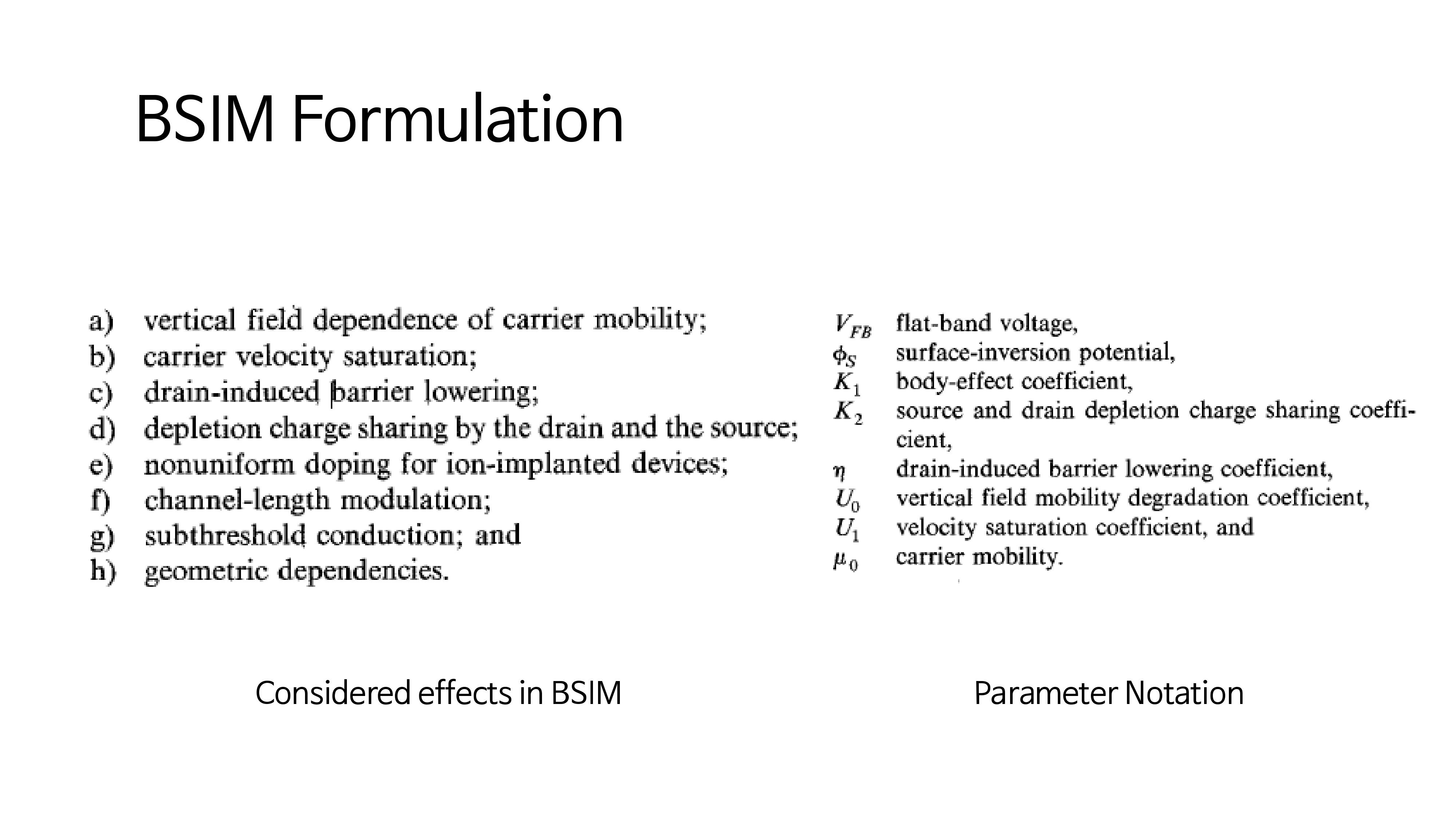
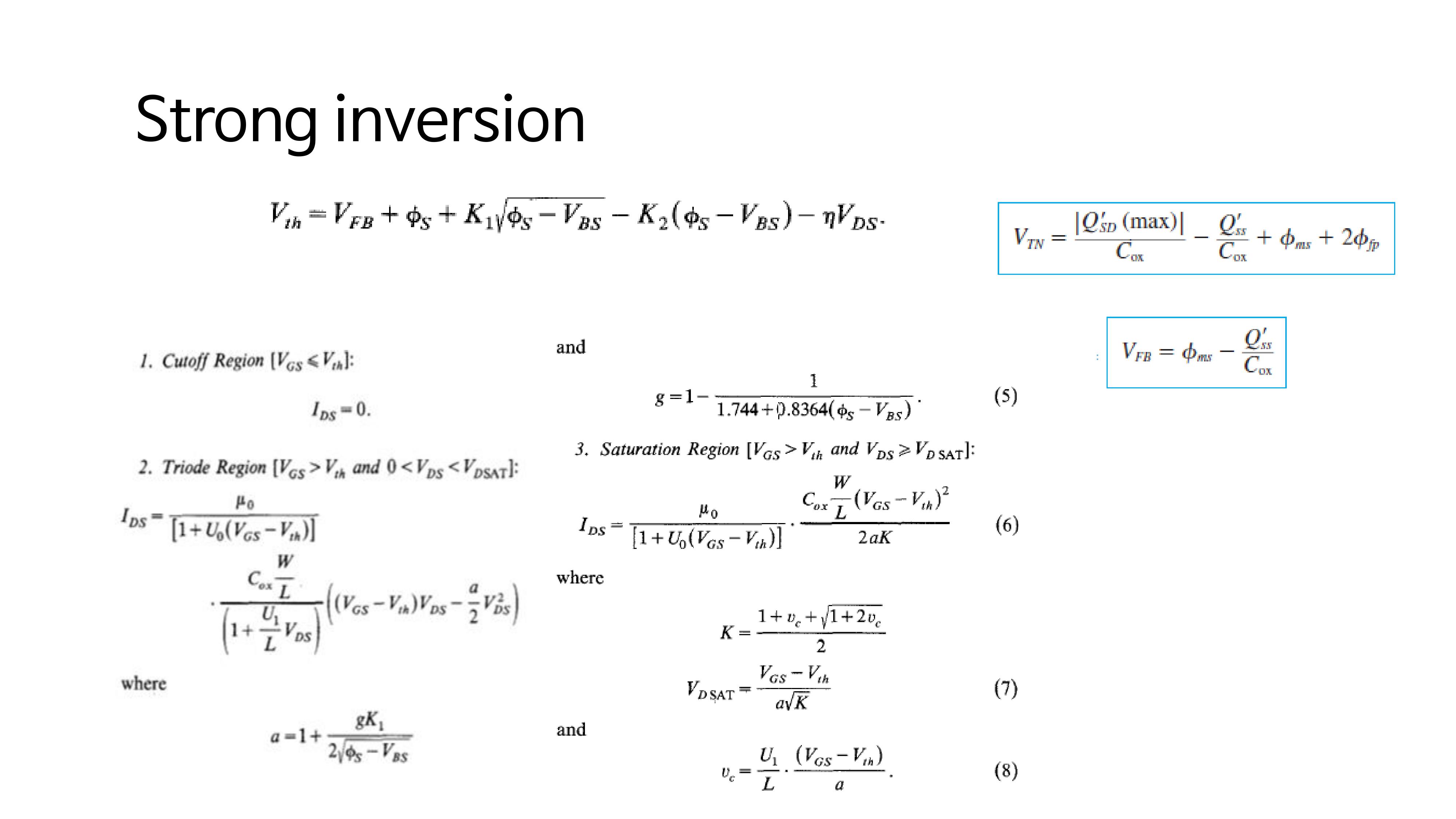
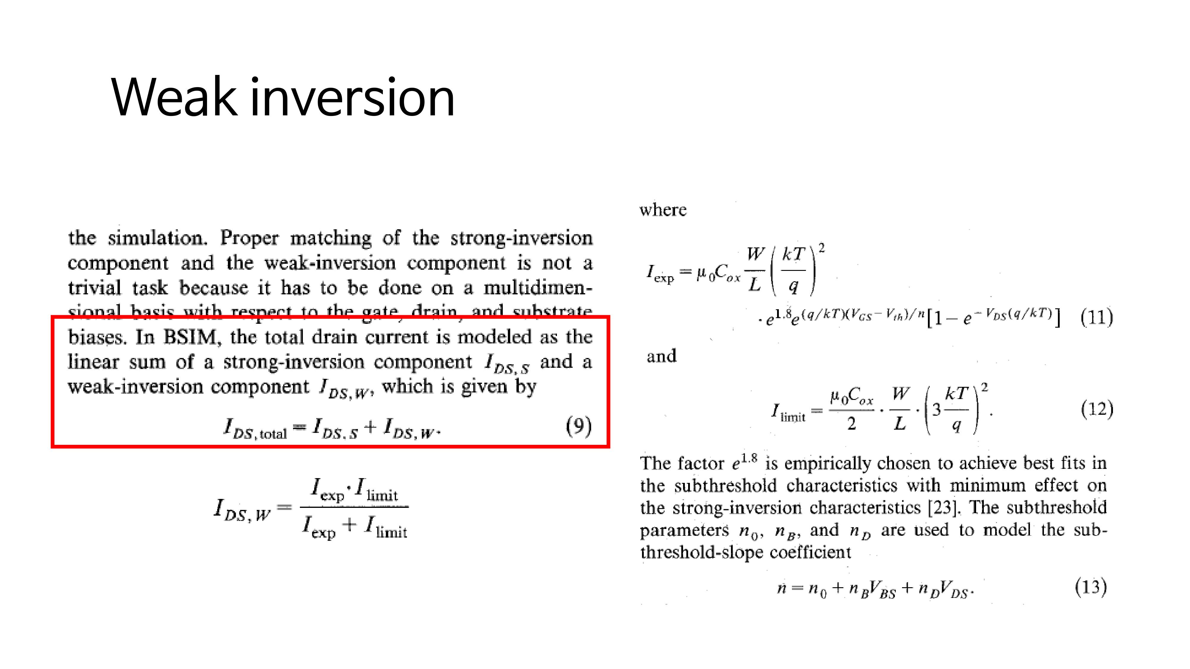
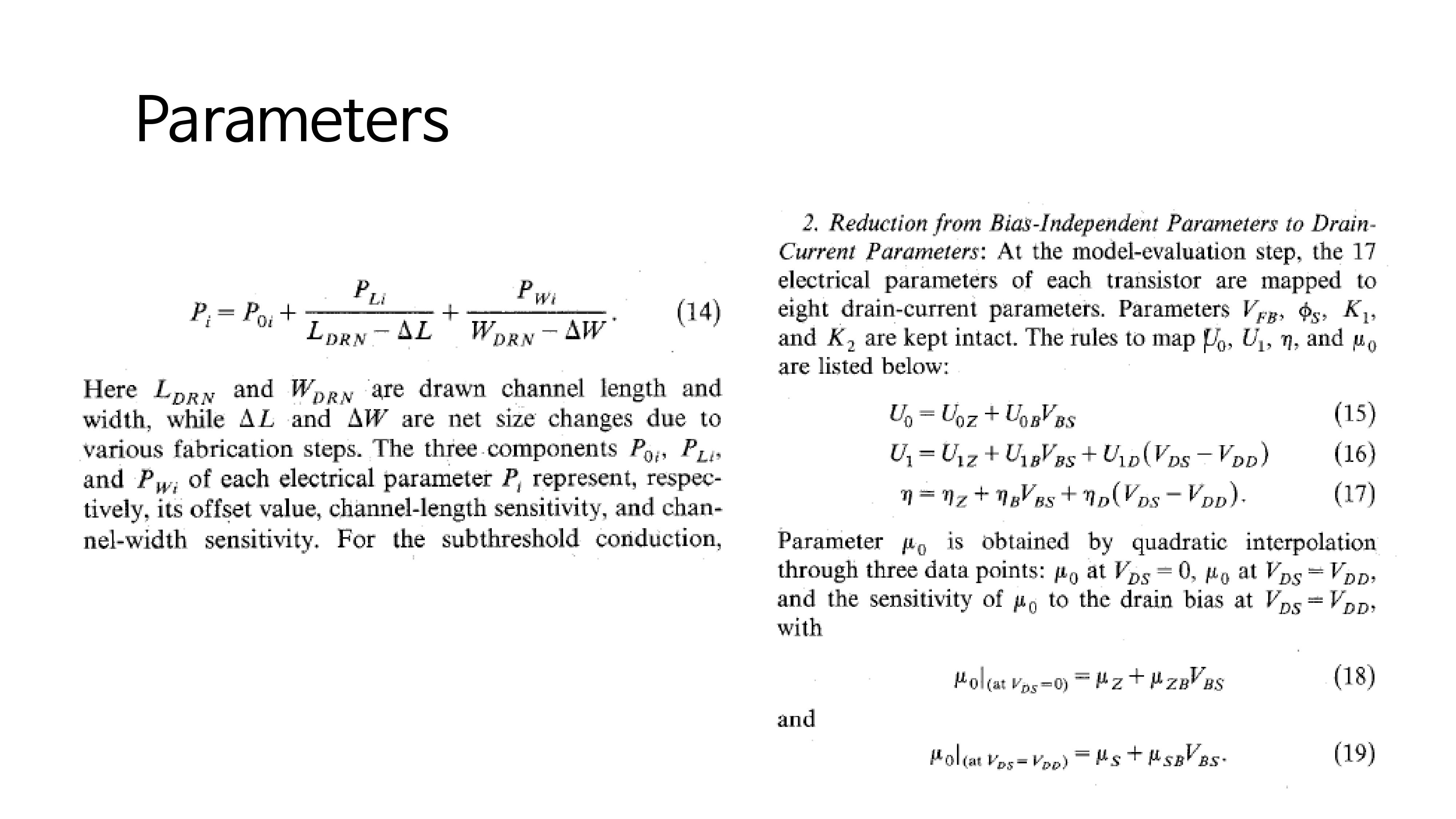
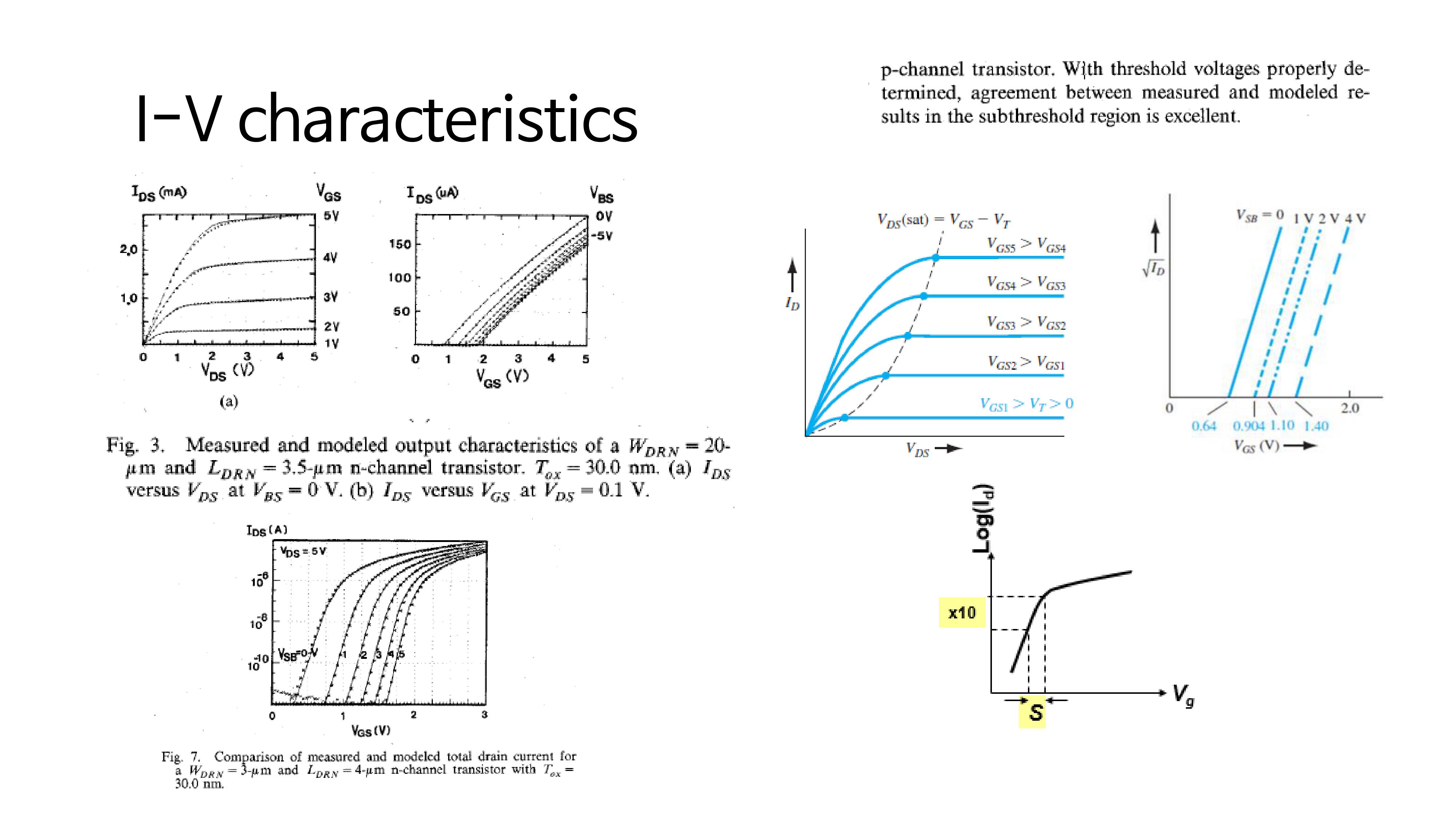
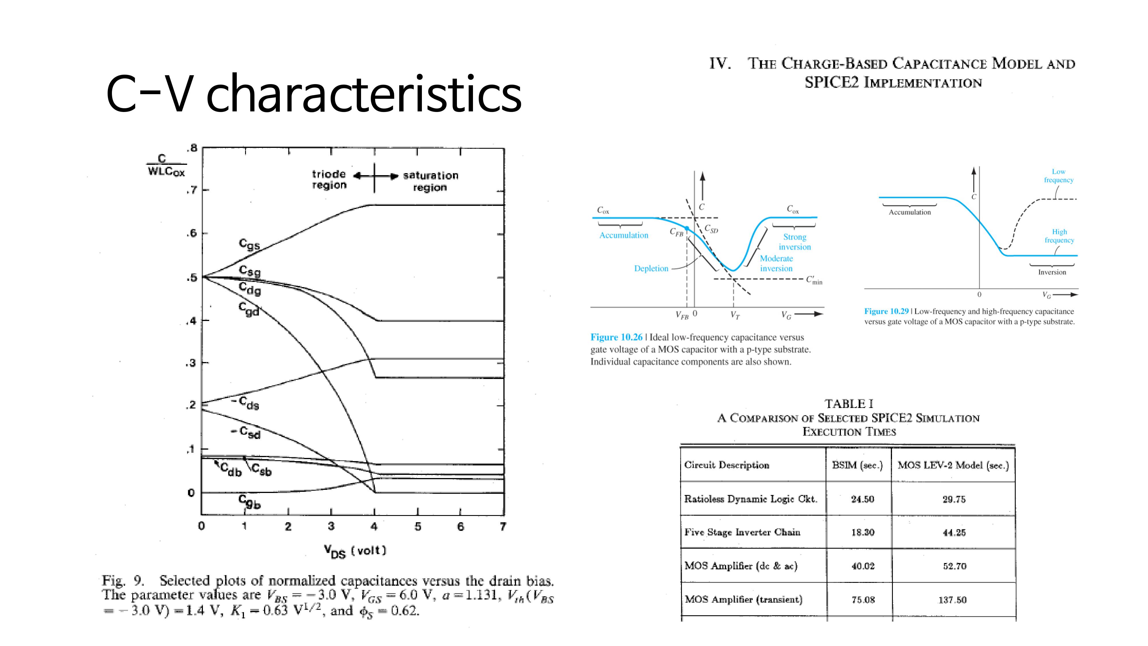 Basic Device Physics Inversion and parameters are defined, and I-V and C-V characteristics are shown. (The figure on the right is the Ideal I-V, C-V curve.)
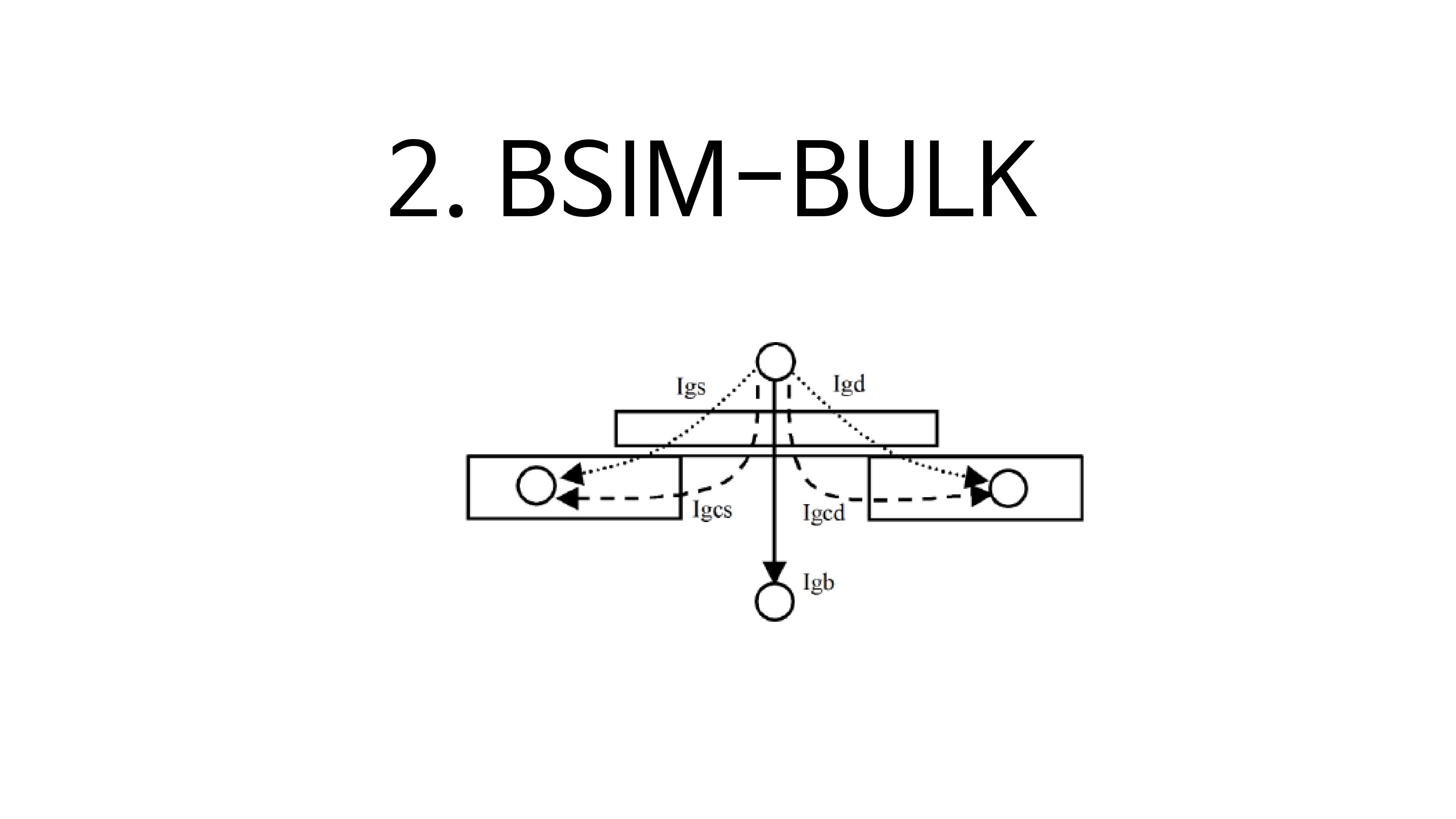 Let’s find out about the BSIM-BULK model.
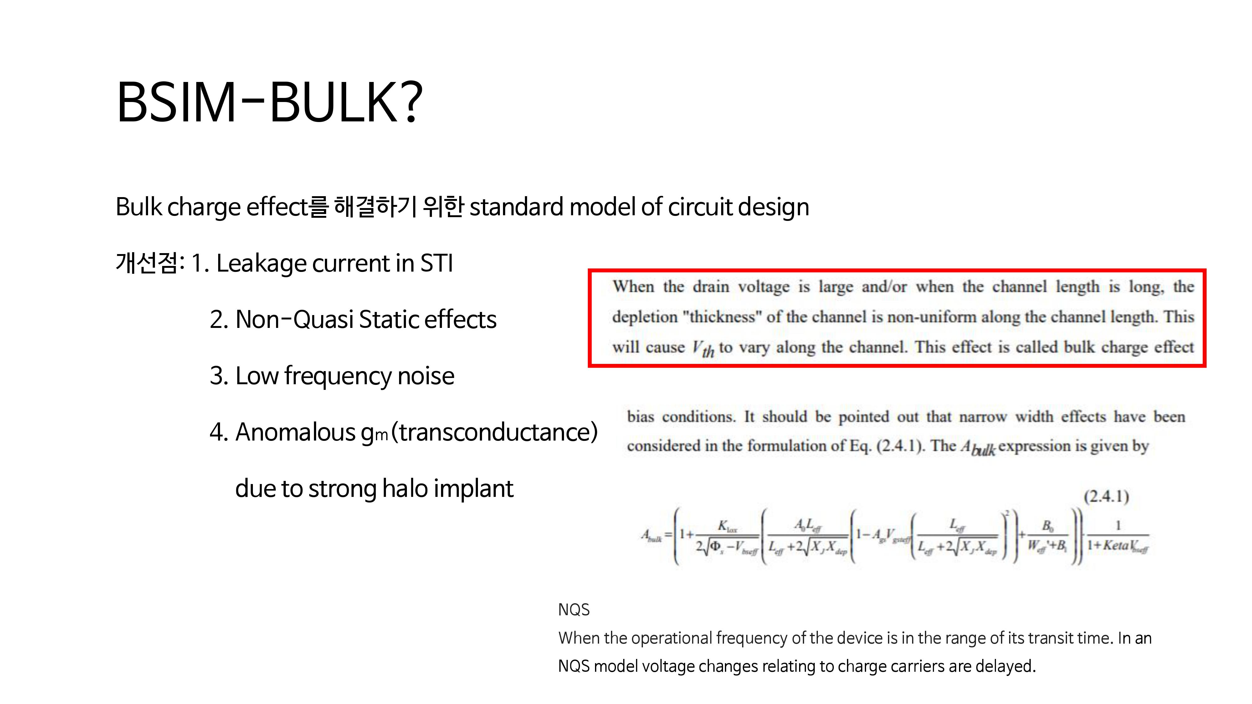 BSIM-BULK is a model for solving the bulk charge effect. The bulk charge effect is a phenomenon in which when the Vd is large or the length of the channel is long, the thickness of the depletion layer appears uniformly, and the threshold voltage changes within the channel. In order to improve this, four major problems such as considering the leakage current in STI are improved models.
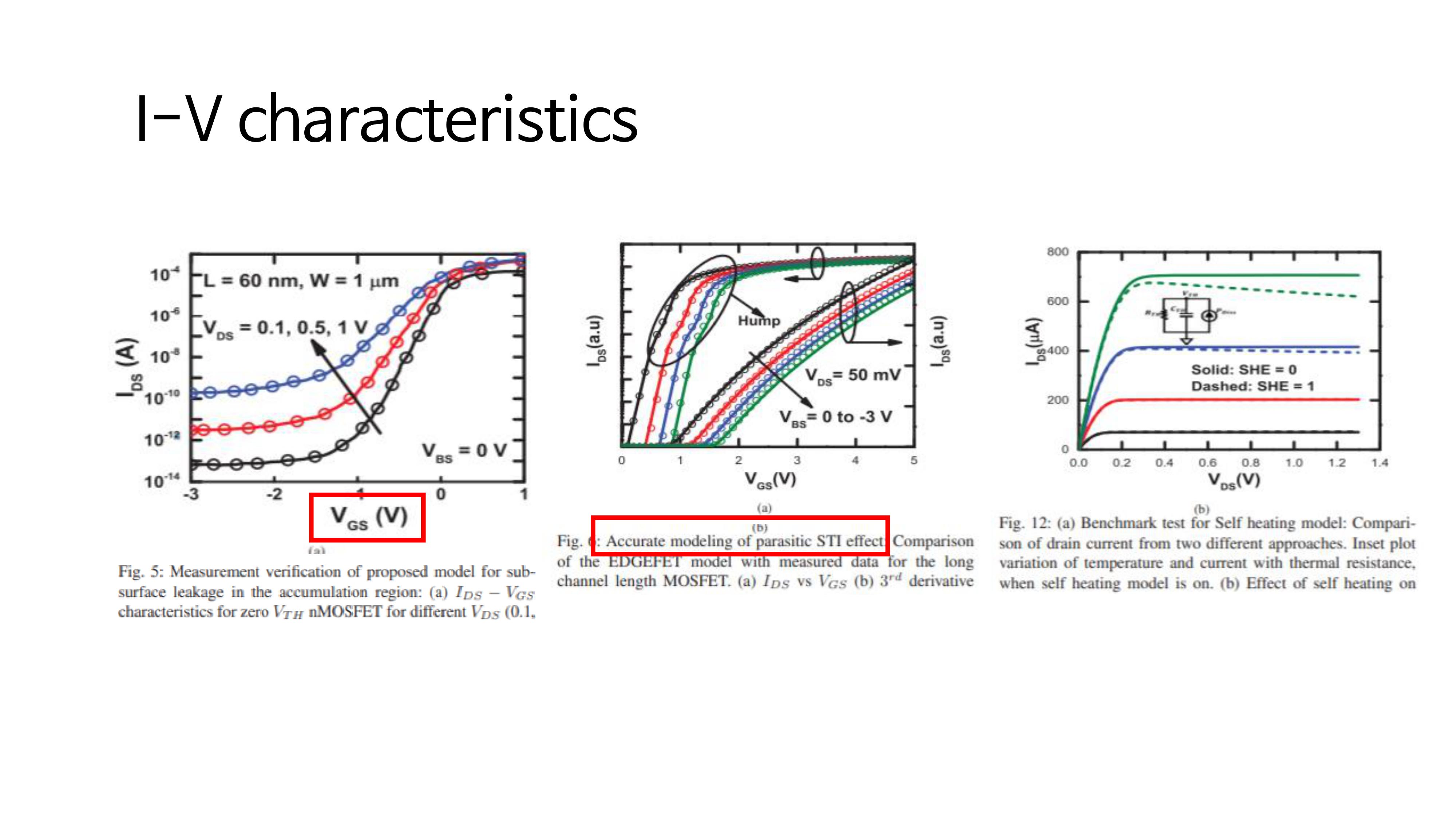
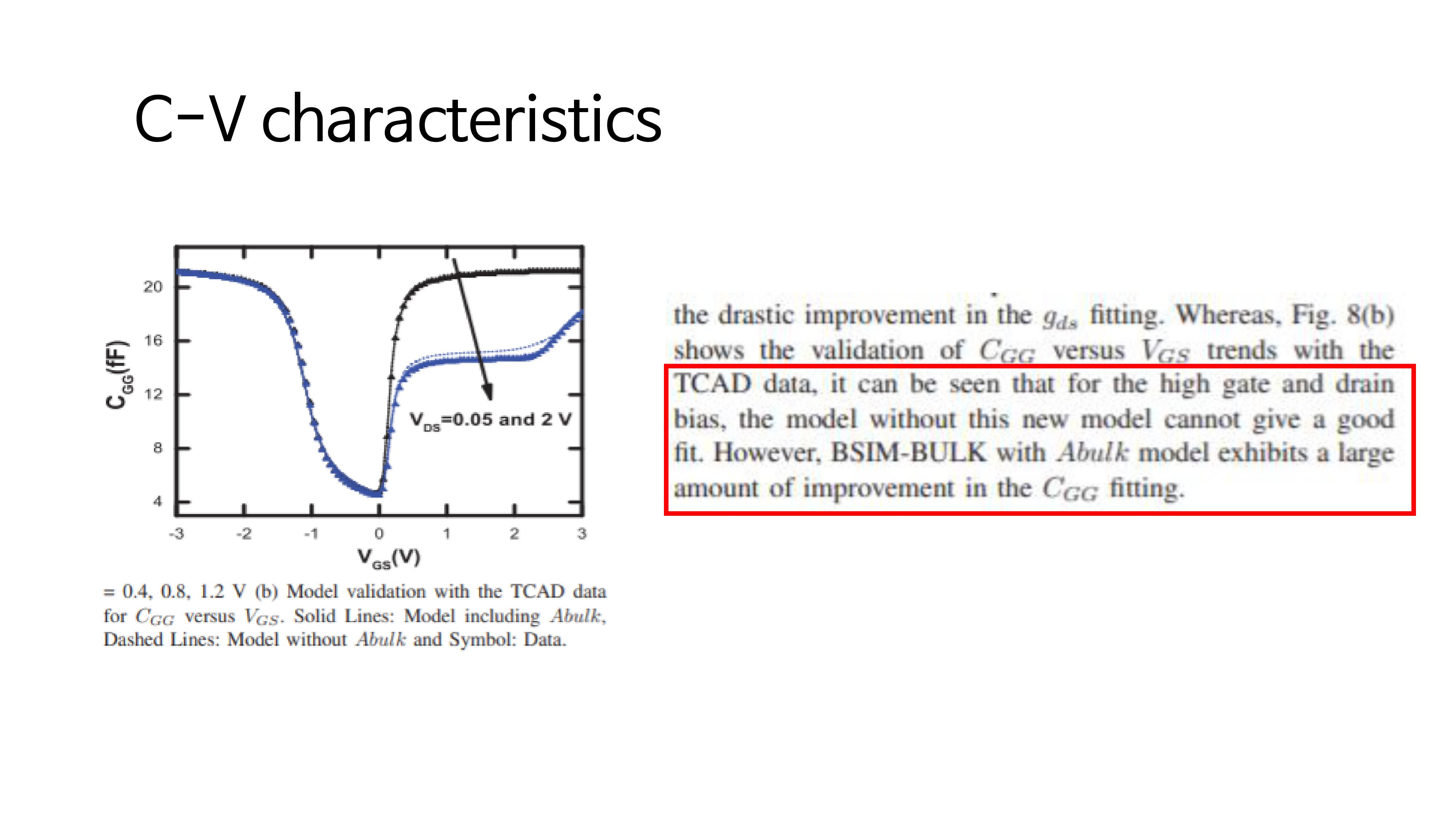 BSIM-BULK’s I-V and C-V curves. In the existing model, a curve did not appear properly in a large Vd (blue), but it can be seen that it comes close to an ideal curve when the BULK model is introduced. (Black curve)
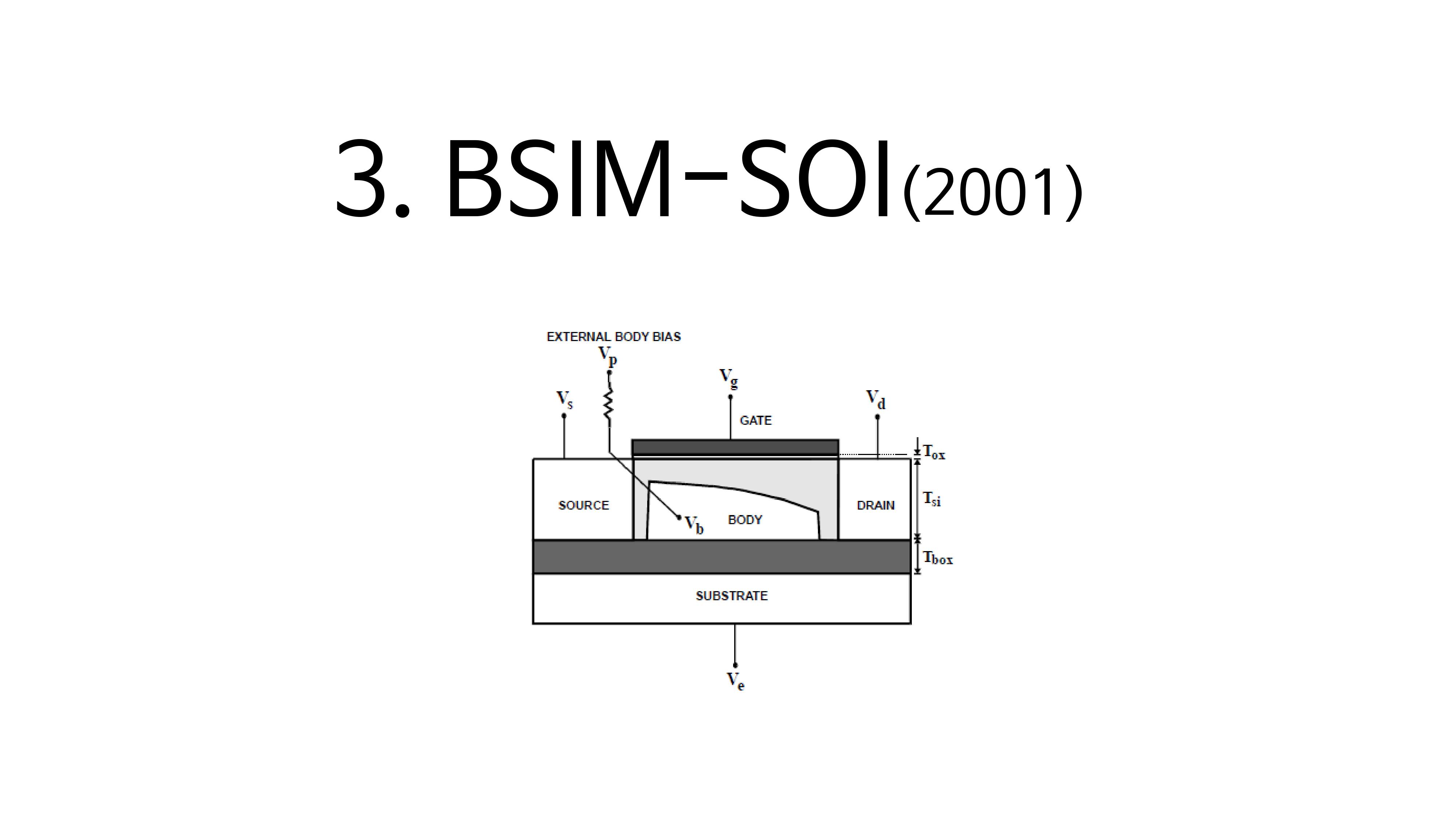 Let’s find out about the BSIM-SOI model
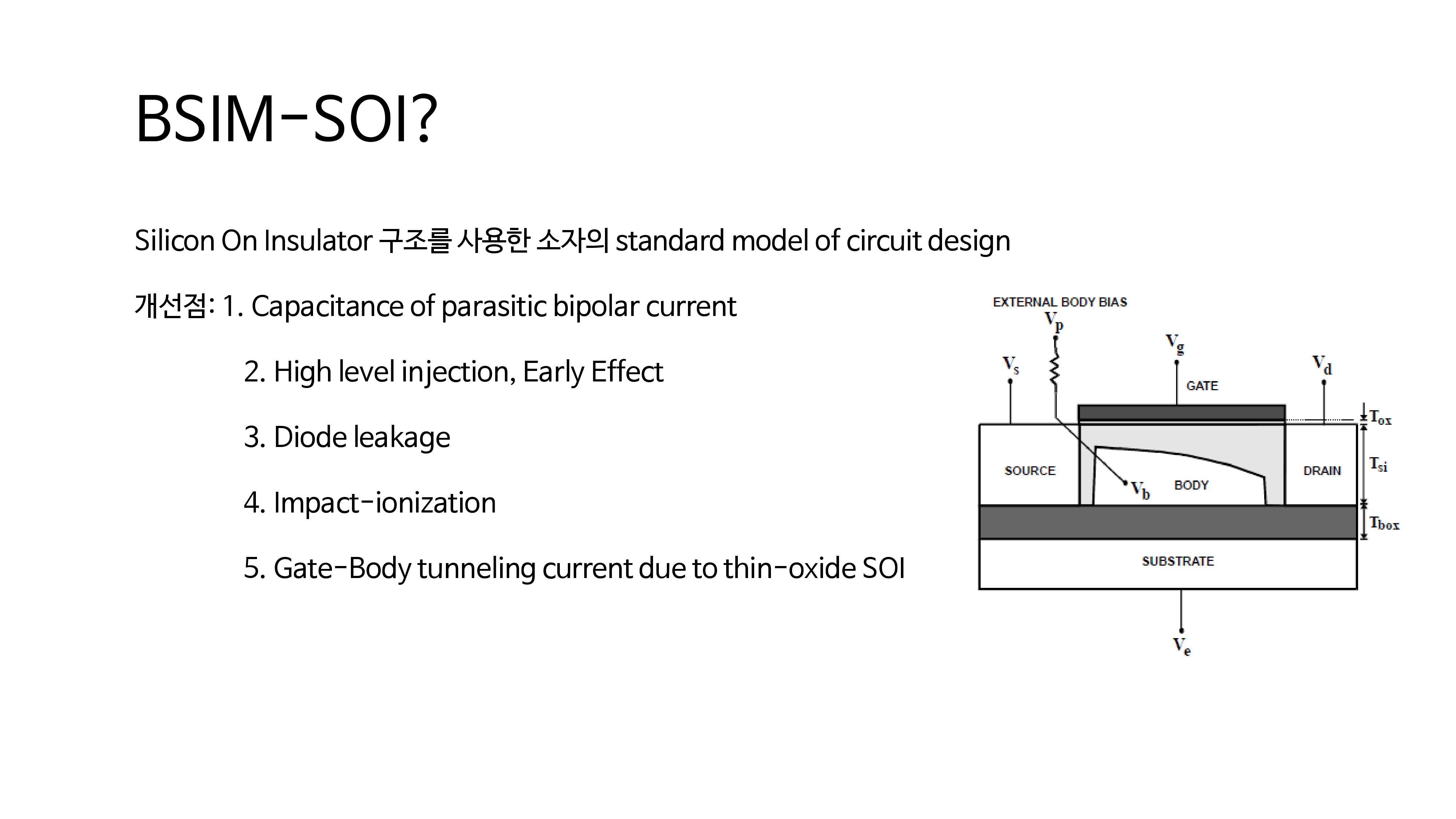 It is a model for modeling a device in a silicon-insulator (SOI) structure that was identified last time. Various problems in Bipolar, such as HLI and Early Effect, leakage current, and Avalanche Breakdown were solved.
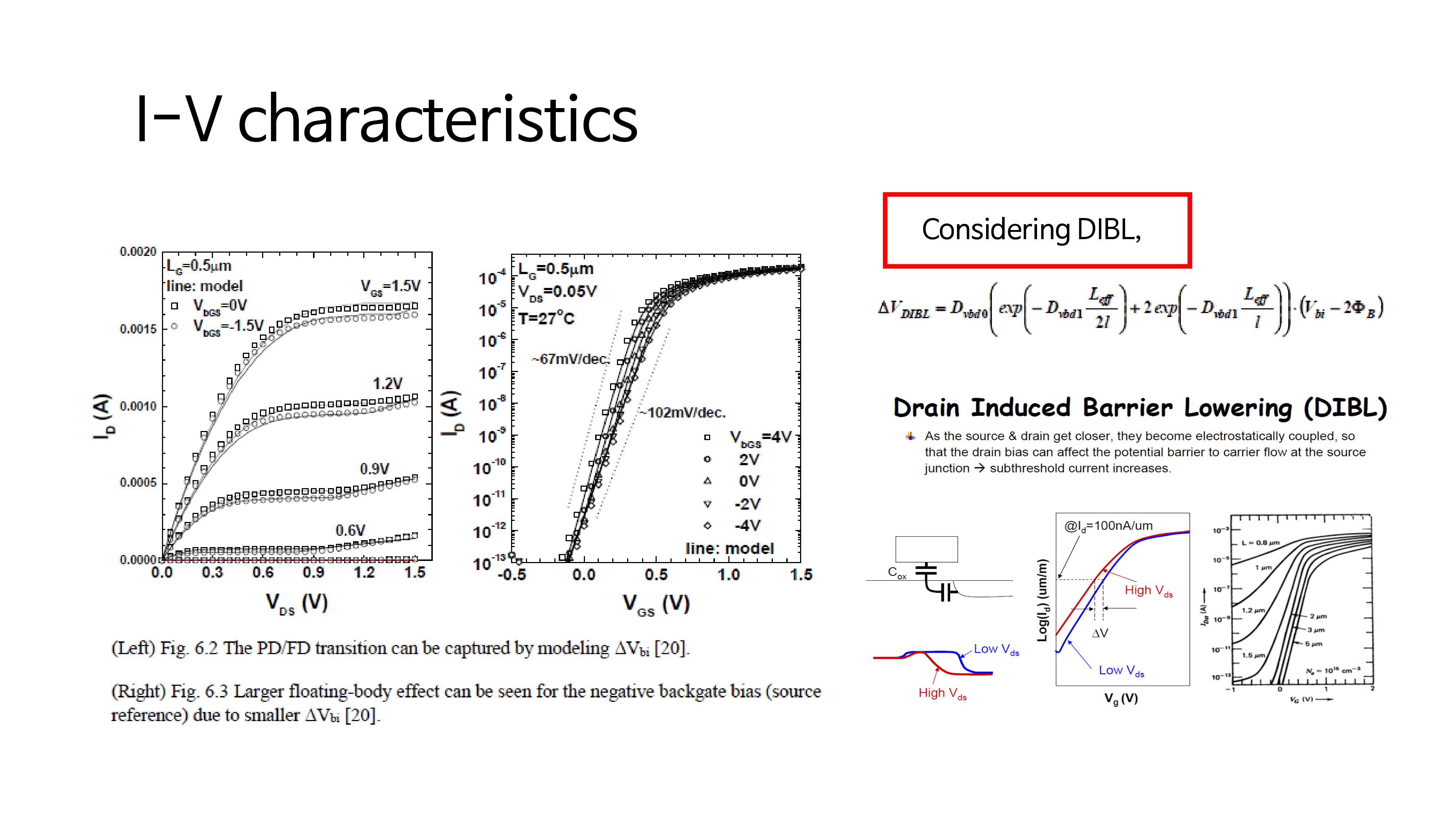
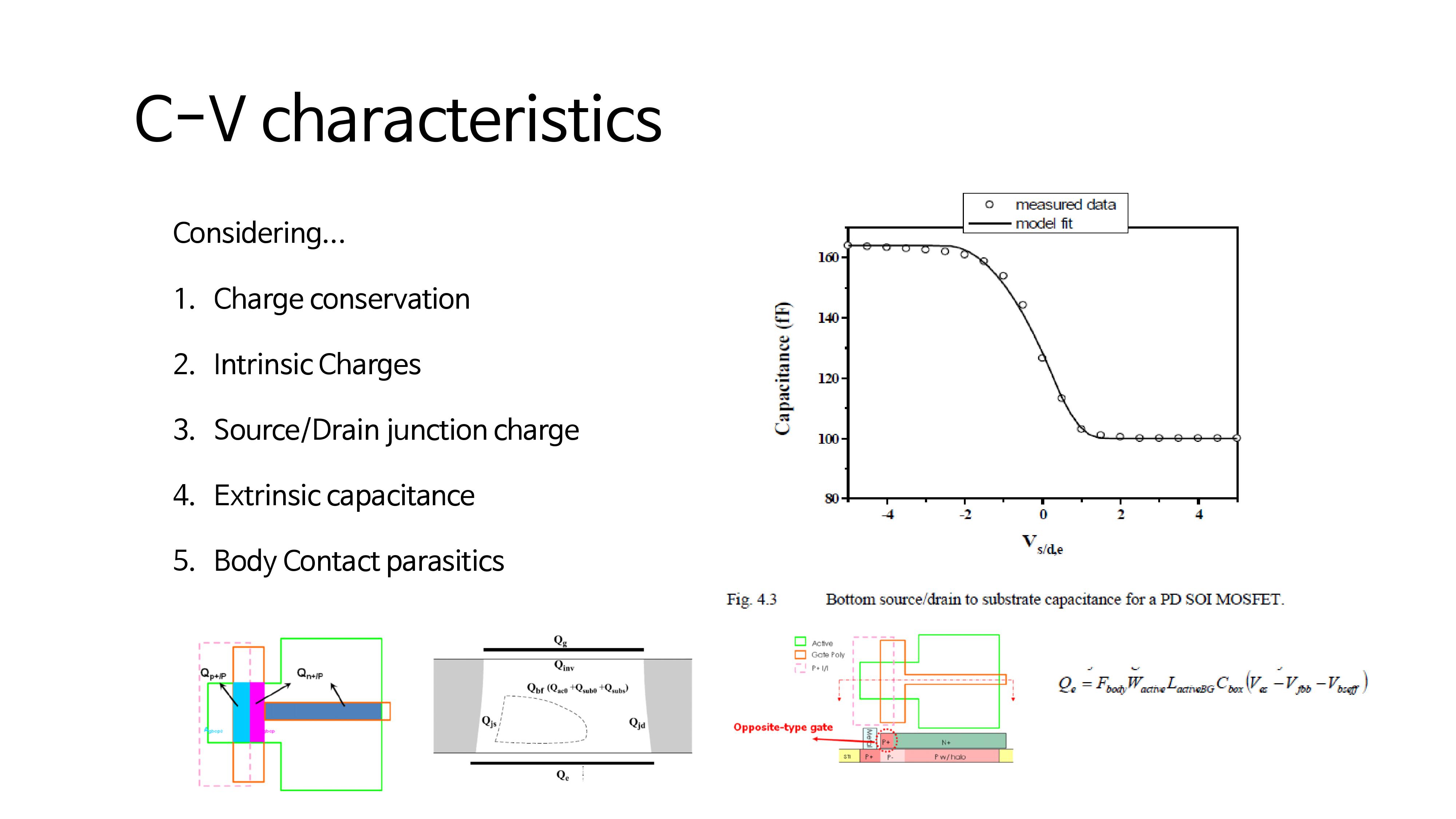 This is an example of I-V and C-V curves of BSIM-BULK. In the I-V char, the curve was drawn in consideration of the barrier reduction effect induced by the DIBL, that is, the drain, and it can be seen that it was close to the ideal curve.
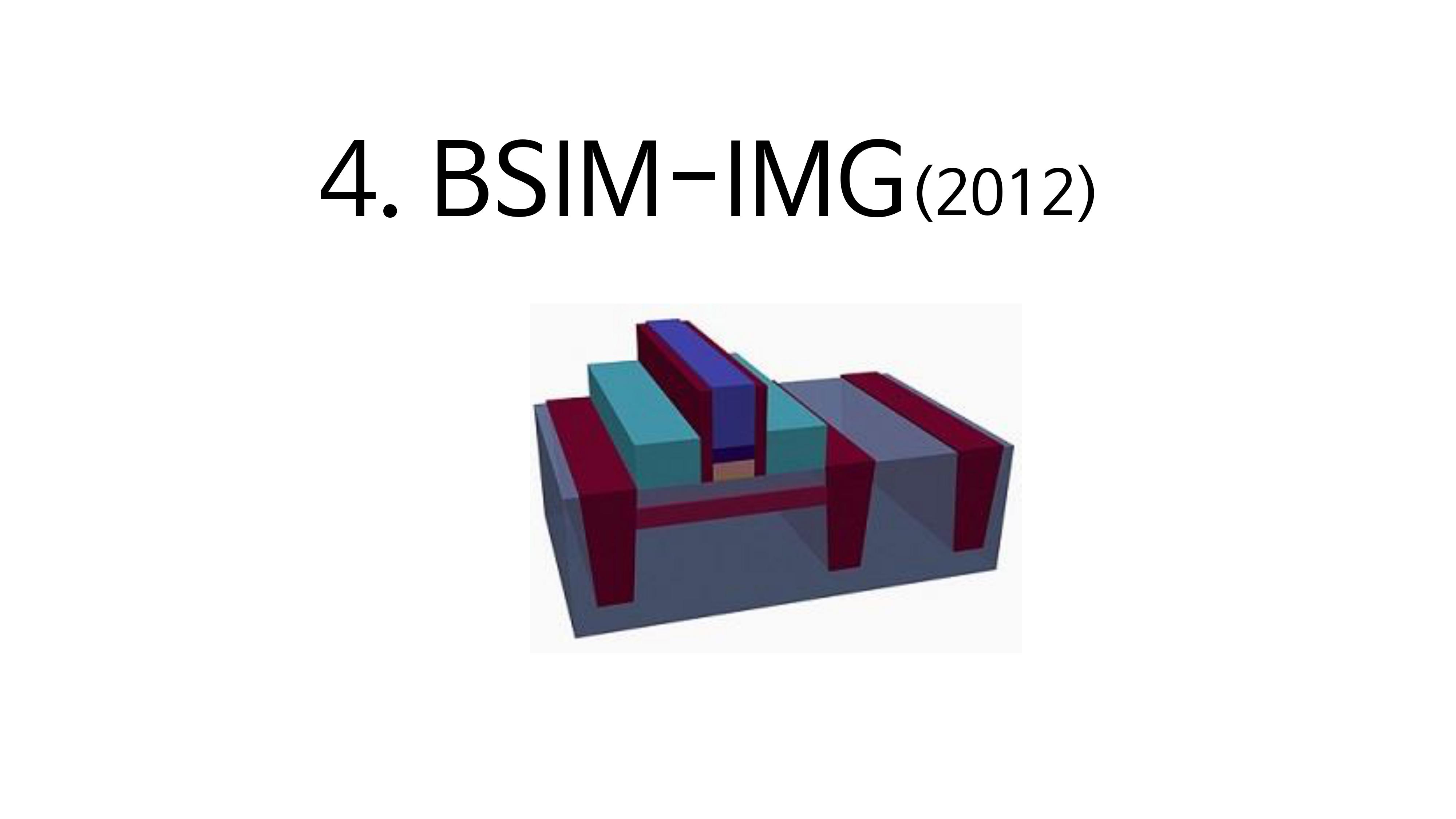 Let’s look at the BSIM-IMG model.
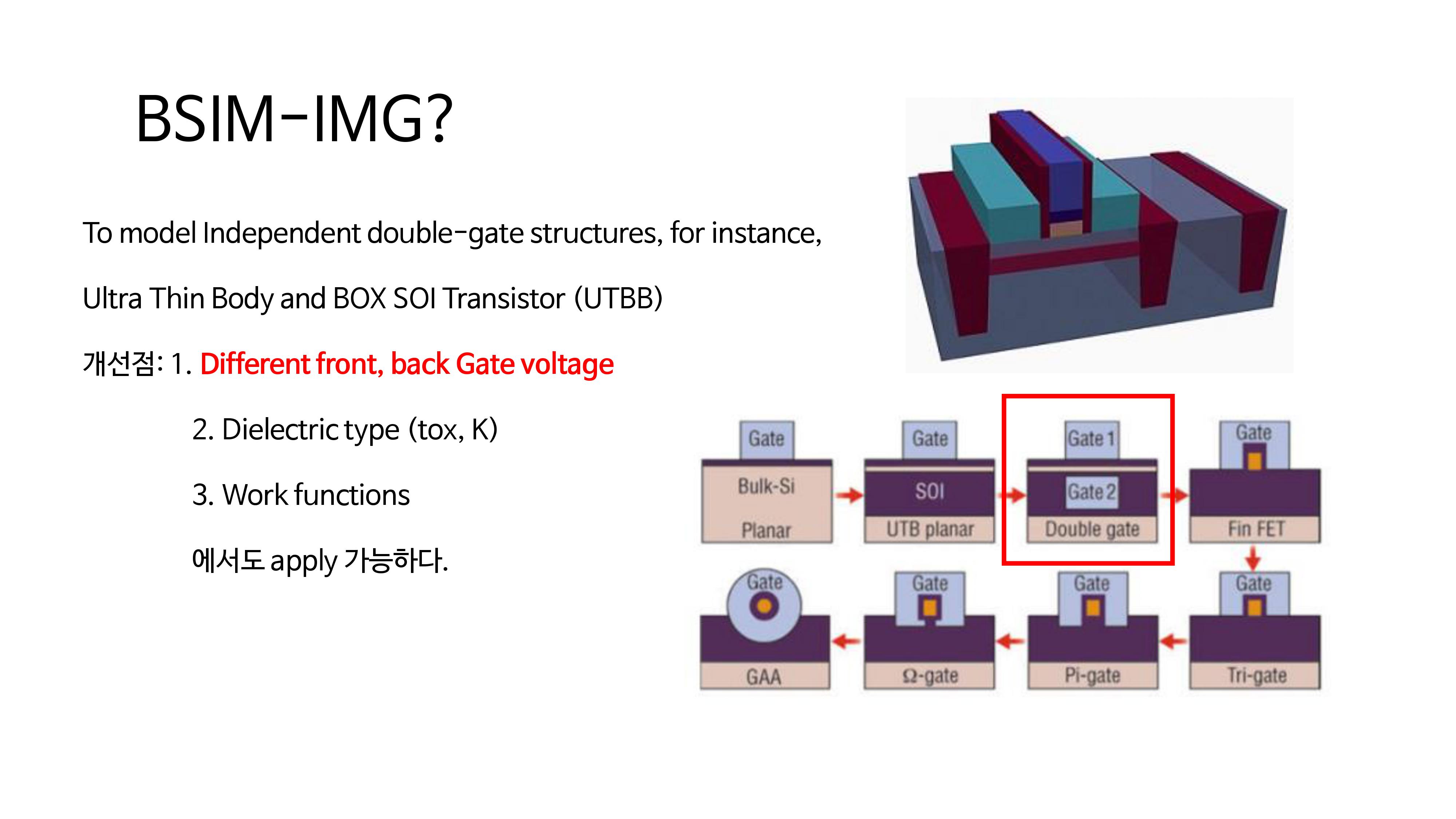 The BSIM-IMG model is intended to model a UTBB, i.e. a two-gate model such as a thin body and a Buried Oxide SOI transistor. What should be noted in this model is that the Front Gate and Back Gate Bias are applied differently, and both the front and back gates’ genomes and work functions should be different in the model.
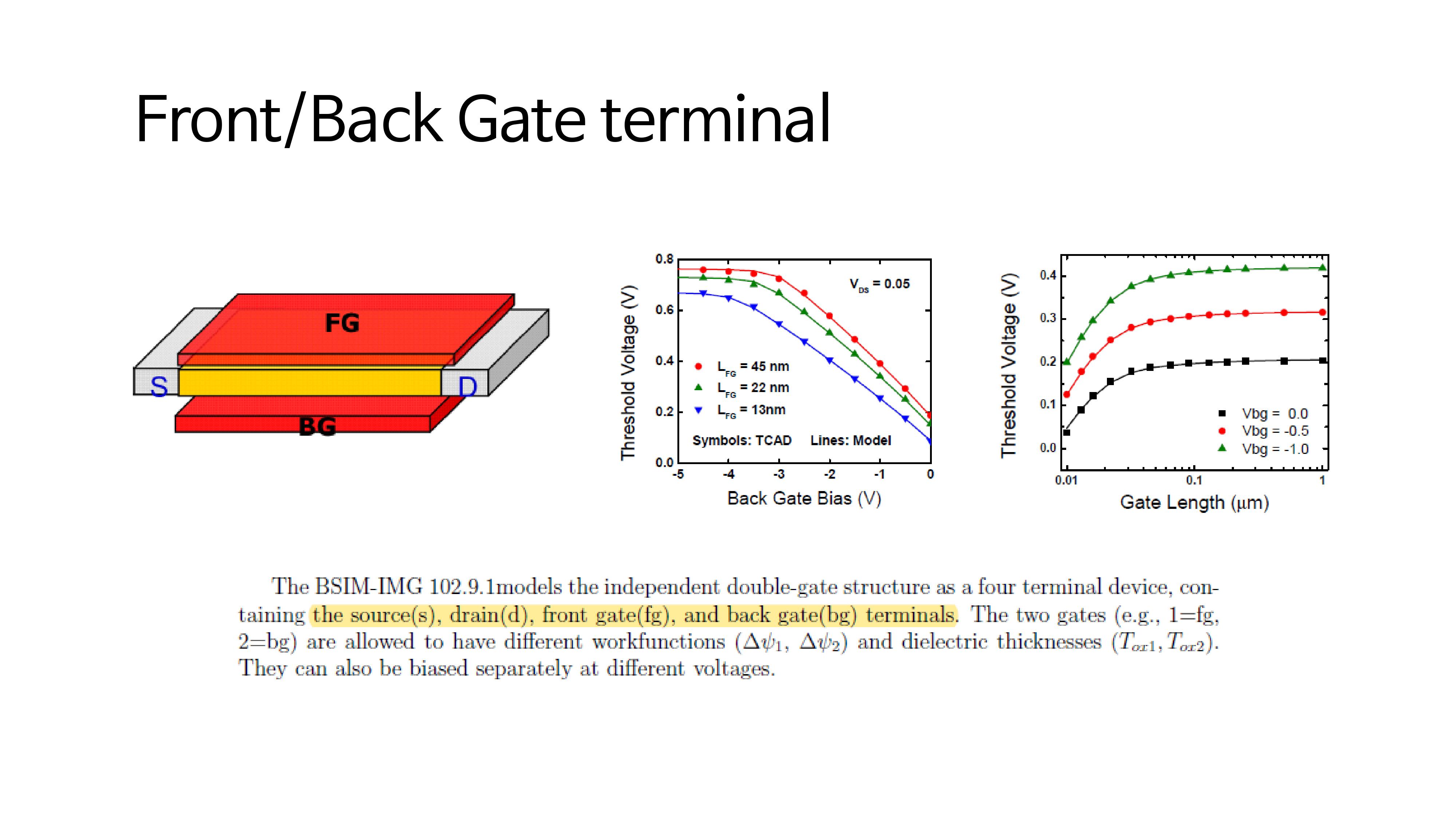 Looking at the figure, it can be seen that the terminal should consider a total of five Bias, Source(S), Drain(D), Front gate(FG), Back gate(BG), and Body(B), as mentioned above.
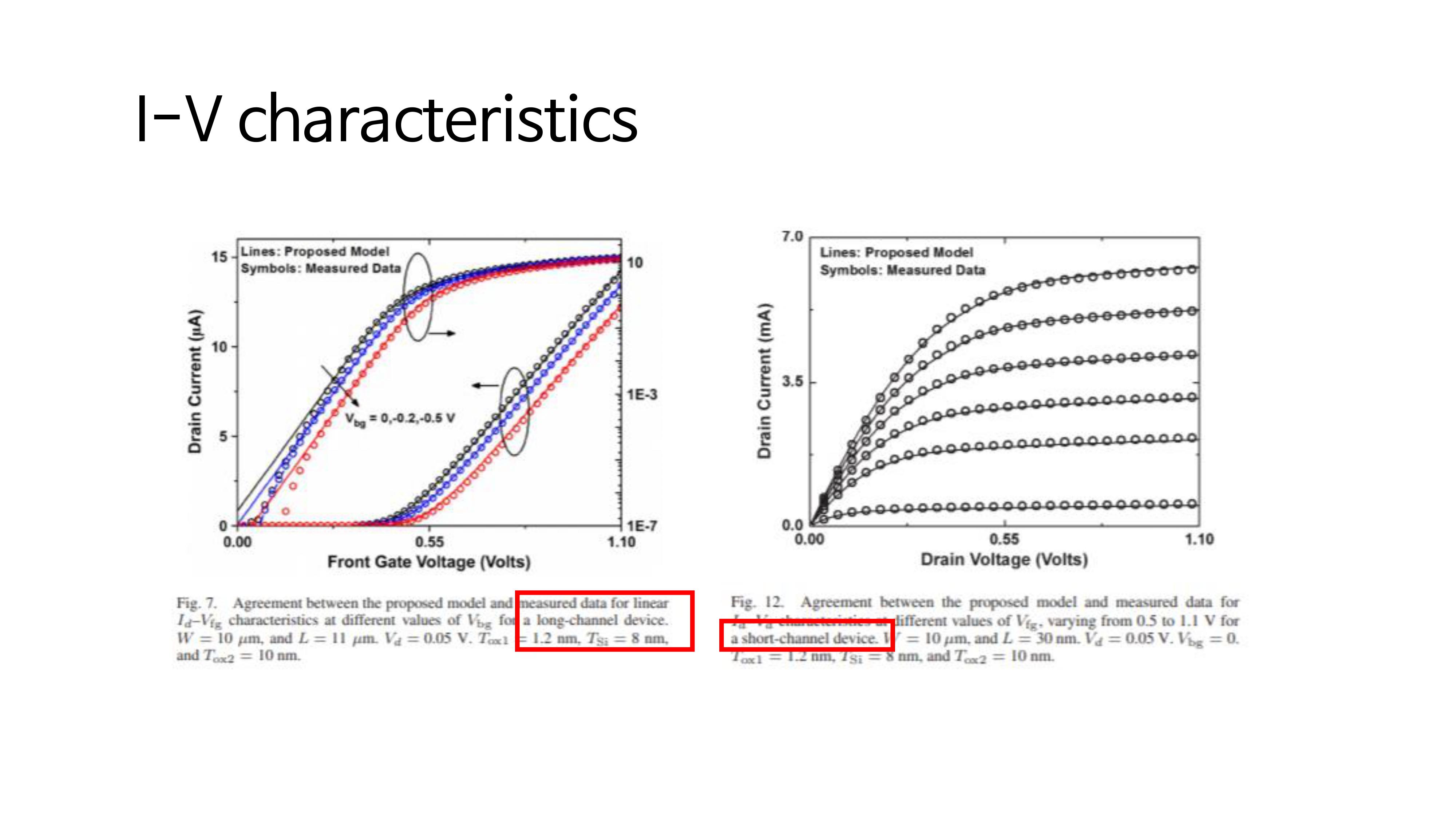
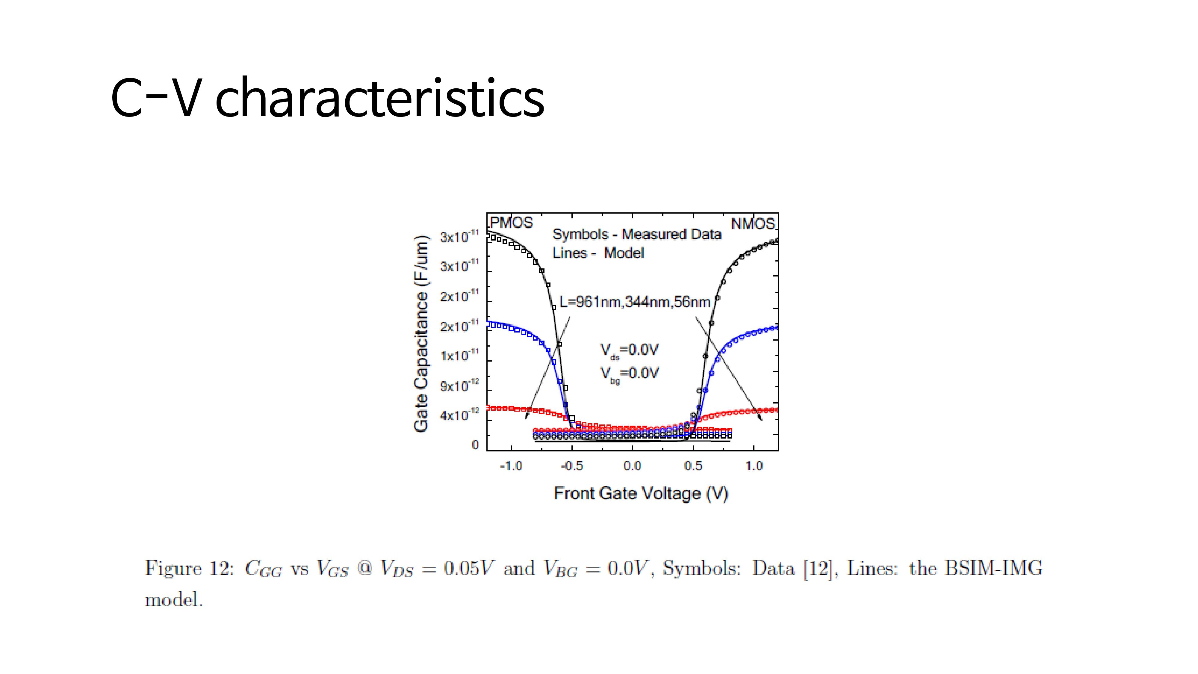 This is an example of I-V and C-V curves of BSIM-BULK.
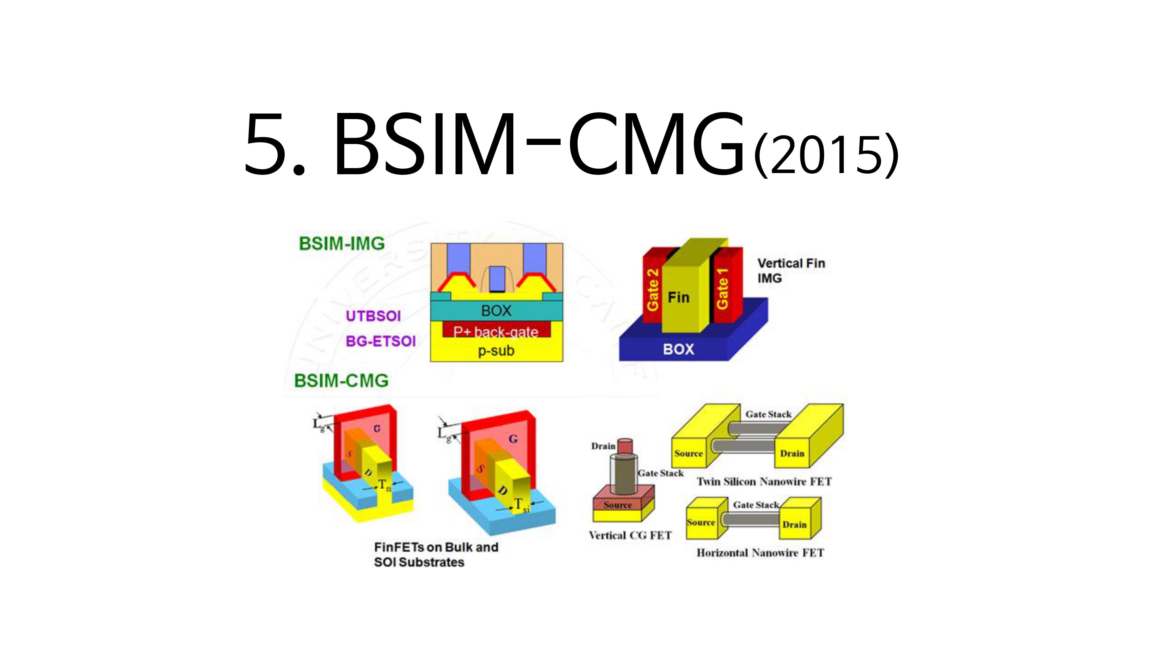 Finally, let’s look at the BSIM-CMG model.
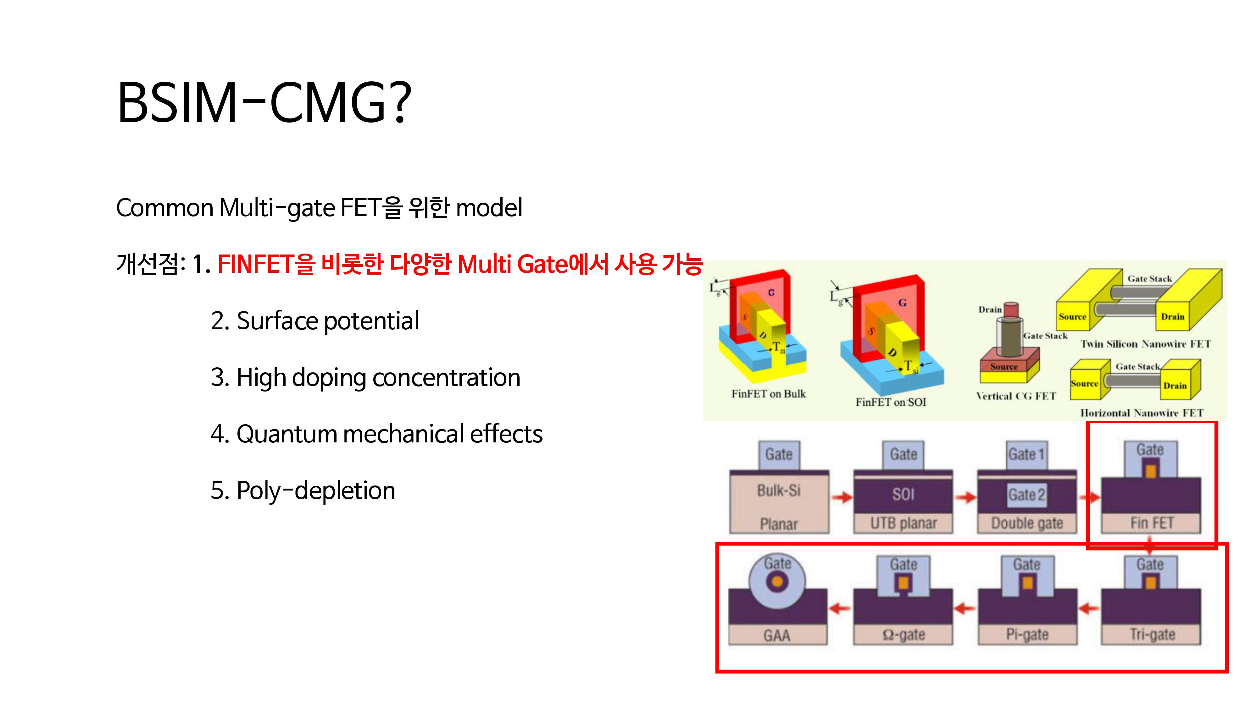 The BSIM-CMG model is a model for the Common Multi-gate FET, which can be used for various multi-gate such as Finfet, GAA, and pi-gate. Additionally, quantum mechanical phenomena, high concentration doping, and surface potential are also considered models.
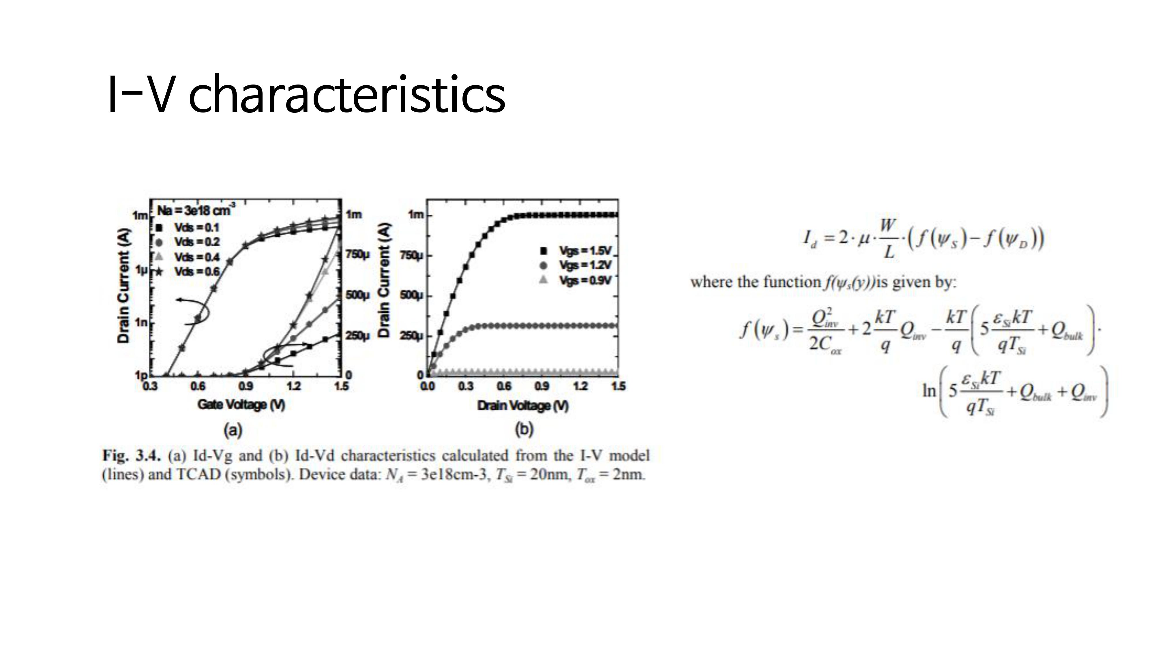
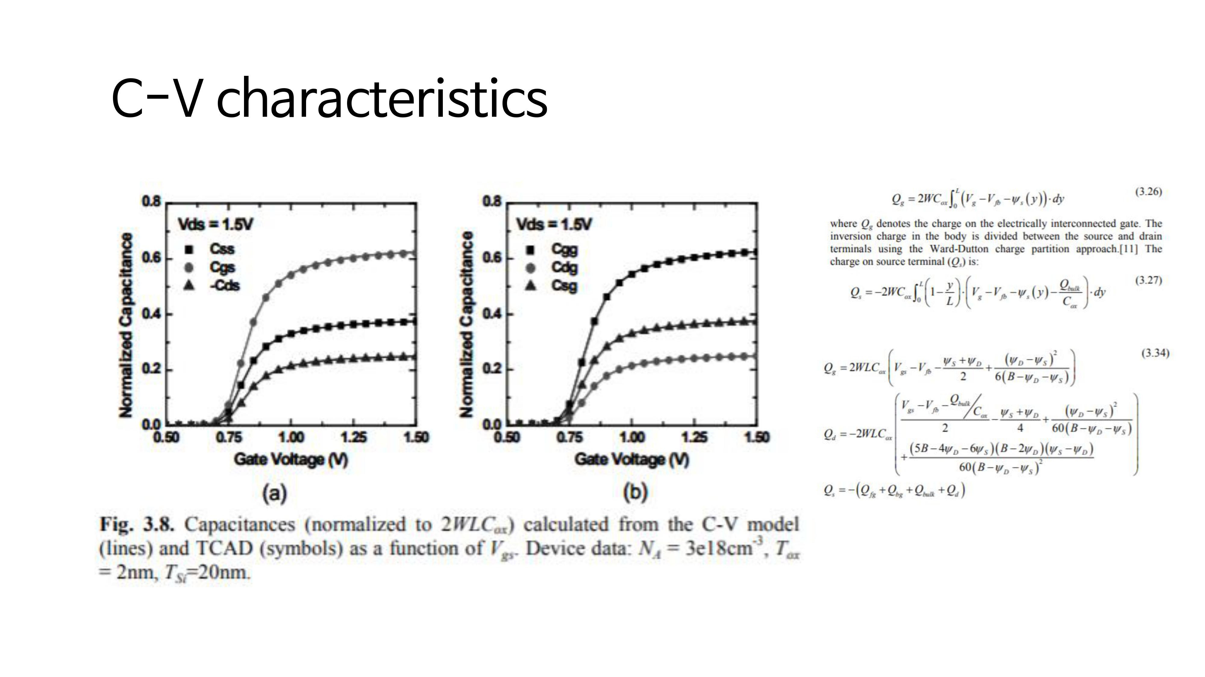 This is an example of I-V and C-V curves of BSIM-CMG.
