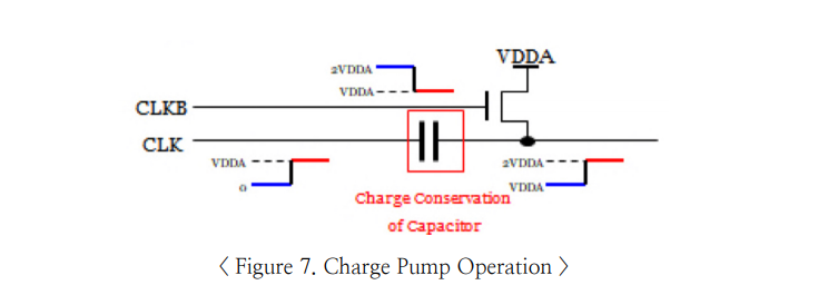
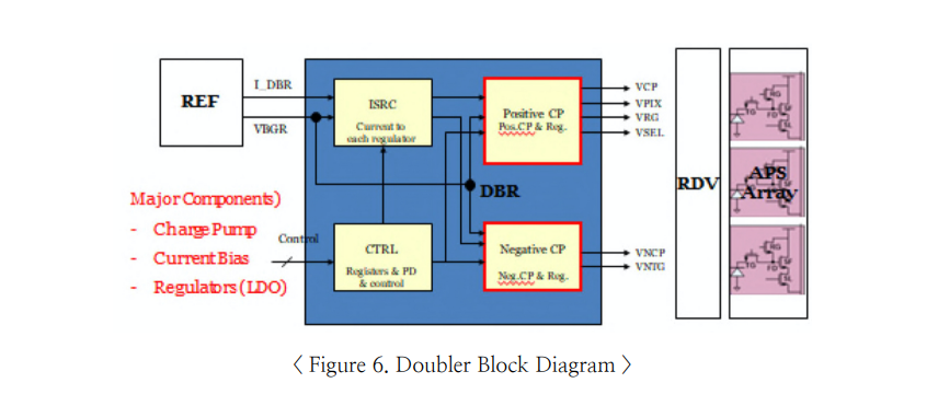
In a CIS circuit, a Doubler is a block that produces a clear voltage of 4.5V, which is about twice as high as the nominal voltage of 2.5V. The most main component of this DBR Block is the charge pump. A charge pump (CP) is a circuit that uses the charge conservation law of a capacitor to generate a higher voltage than a power source. Using these charge pumps makes charge transfer easier on Pixel and can show better performance at the dark level or power immunity.
The Doubler Block consists of Charge Pump, which forms the aforementioned high voltage, a current bias for pump operation, and Regulator (LDO) for clear output voltage formation. This charge pump can also be divided into a positive charge pump forming +4.5 V and Negative CP forming -4.5 V. Basically, the V_NTG that forms the Negative Bias requires a lower value than the Positive, so unlike the PCP that do the pumping only once, it pumps twice and up to three times.
This Single Slope ADC extracts data by comparing Analog Ramp formed in Digital Code and DAC through a comparator and Correlated Double Sampling (CDS Operation) to compensate the lots of mismatch as aformentioned. The DAC, i.e., Ramp Generator, that generates the Analog Ramp used in these comparisons must also be accurately designed to work properly without errors. In addition, RMP can act as various functions such as analog gain control or ADC saturation level adjustment, so accurate design is required. Rather than improving the performance of this Ramp Generator, this project proceeded to understand Ramp Block by studying the principles and performance factors of the Ramp and analyzing existing designed circuits and simulations.

This project was conducted in the direction of modeling the charge pump with loss resistance, measuring loss, analyzing the circuit, and improving it. The performance of CP can be expressed as Rs and Power Consumption. First, Rs can be obtained by dividing the Voltage Drop generated by the Charge Pump by the Load Current, and the lower this Rs, the less loss occurs, that is, the more efficient the Charge Pump. Power consumption can be obtained by multiplying the load current over the entire Nominal Voltage, which is also thought to have better performance if it is lower.
The simulation focused on performance changes according to a total of two factors. First, we examined the improvement results of the Performance Index according to the clock frequency of CP. As a result, the following results and the resulting physical causes could be derived:
1. Sizing
1.1. The larger the chip size, the lower the Rs, but the higher the power consumption. (Trade-off): Voltage drop by load current increases when NMOS (Lower Switch in NCP) size becomes smaller, Rs increases, and efficiency decreases. Also, If the PMOS (upper switch in NCP) becomes smaller, the time constant when charging the cap increases, thus refresh cannot occur in time, and efficiency decreases, that is, increasing Rs.
1.2. Power efficiency degradation occurs when Switch Tr is too large compared to Flying Cap: If we extract the data into Excel and differentiate the plotted graph, we can obtain the result as follow: the Switch Transistor’s length gets larger, and the power consumption grows in quadratic order.
2. Frequency
2.1. The higher the CP Clock Frequency, the lower the Rs, but the higher the power consumption: The equation modeled on the Charge Pump shows that the frequency is inversely proportional to the Voltage Drop, so Rs decreases at high frequencies. In addition, since high-frequency clocks require more Consumption, the increase in Power Consumption can be said to be self-evident.
2.2. The smaller the PMOS size, the lower the high-frequency efficiency and the higher the low-frequency efficiency. Defining and plotting the Rs reduction ratio according to the double increase in PMOS width as ‘etha’, it can be seen that ‘Ehta’ is large at low frequencies and small at high frequencies when PMOS size is small.
