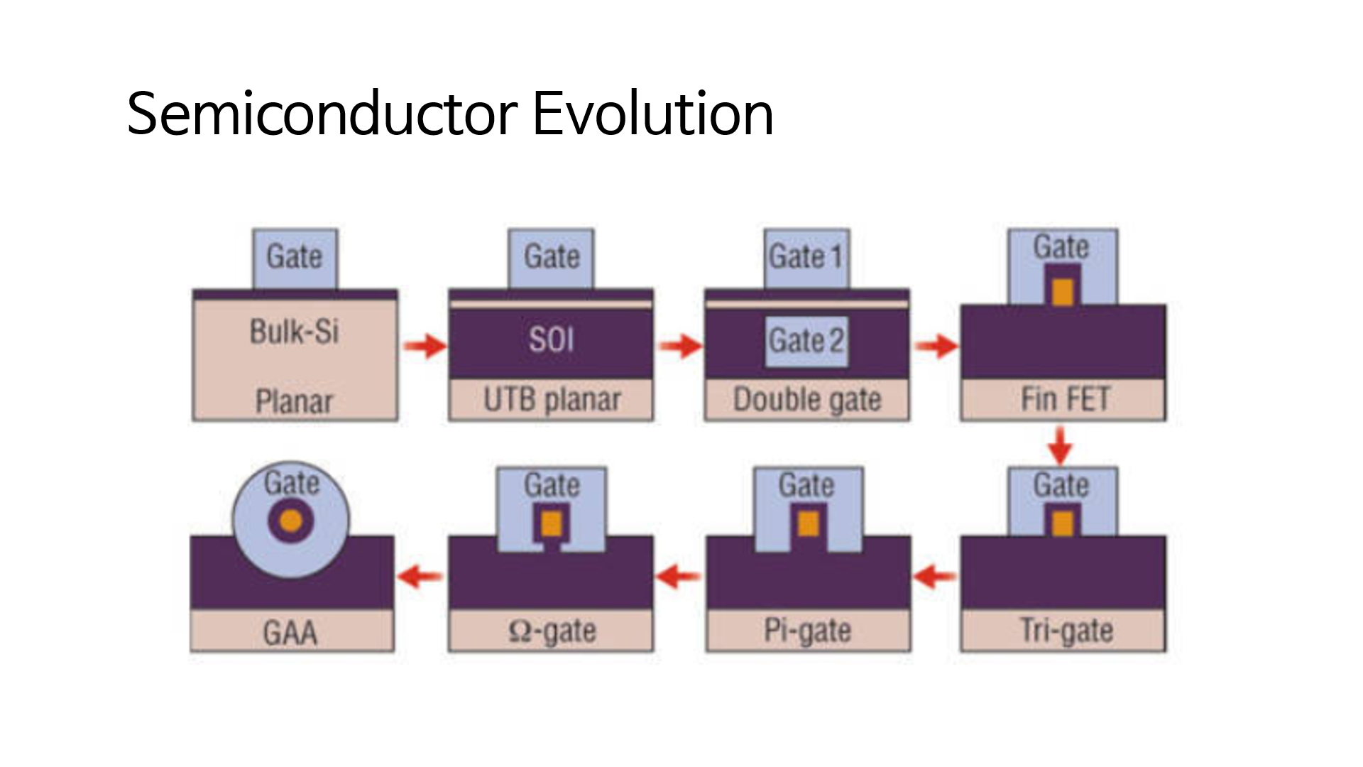
Smaller devices are needed to achieve faster and higher yields. However, due to various matters such as DIBL, punch-through, SS, and Hot Carrier Effect caused by Short Channel Effect, we need to find a way to solve this Short Channel Effect. Engineers attempted material changes in Planer MOS in a material science way, such as widening the gap between High-K and silicon lattice. However, there is a limit to this, so it was decided to change the shape of the FET altogether.

As the recent generation progresses, the area that Gate surrounds the channel increases. Today, let’s take a look at FinFET and GAA, which are being commercialized and will be available.

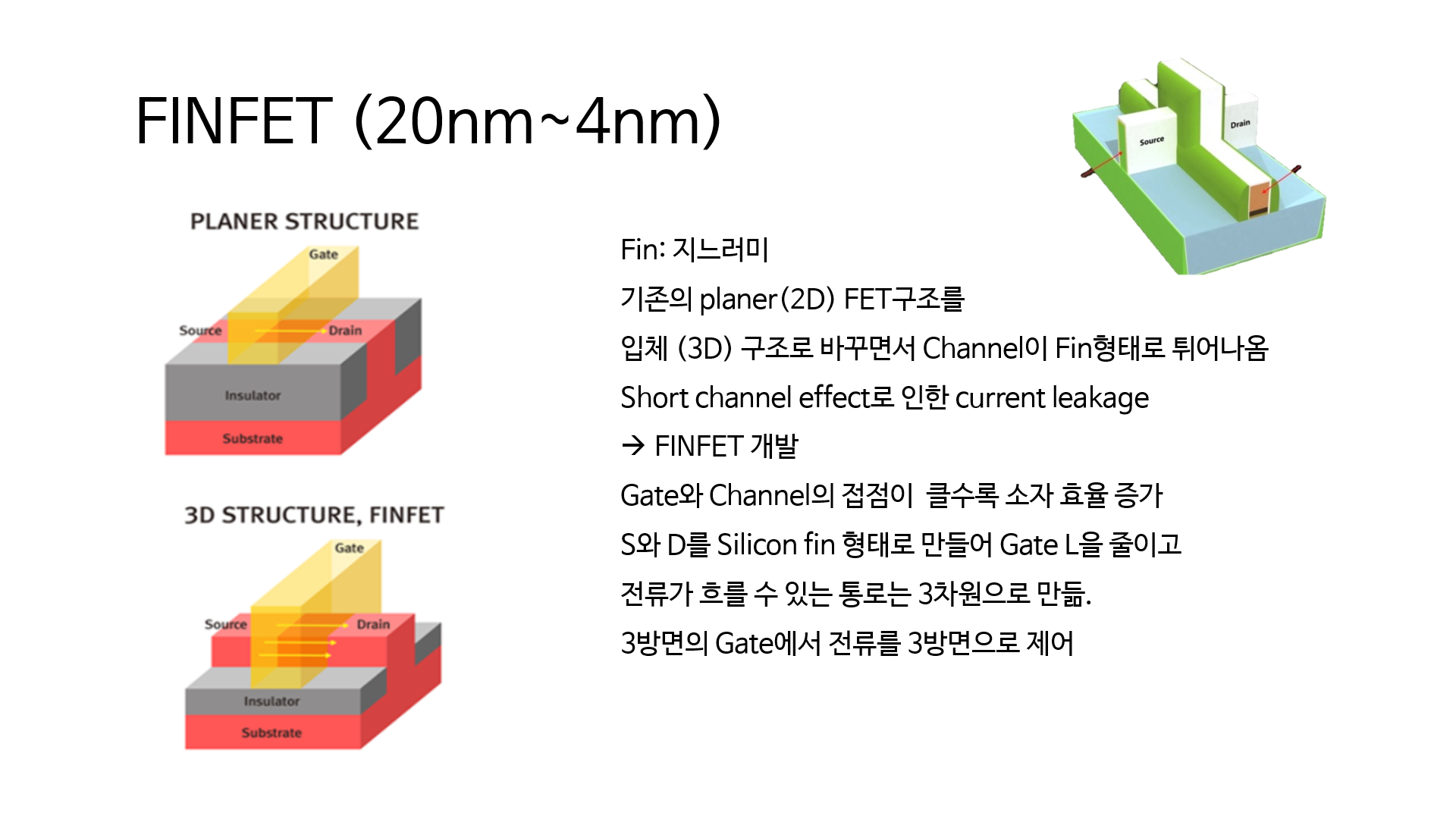
Fin is a term for that of fish’s fin, and can be conceived of shark fin shark-fin. It was developed to solve the current leakage caused by the short channel effect as a device that protrudes into a fin shape while changing the FET structure, which is the existing 2D planner, to a three-dimensional structure.
The larger the contact point between the gate and the channel, the more efficient the device is, and the FinFET structure reduces the length of the gate by making the source and drain in the form of silicon fins, and controls the current in three dimensions at the gate. A short channel effect that cannot be controlled by Planer FET from 20nm appears, and FinFET is actually used for processes below 20nm process. In theory, FinFET can be used up to 4 nm.

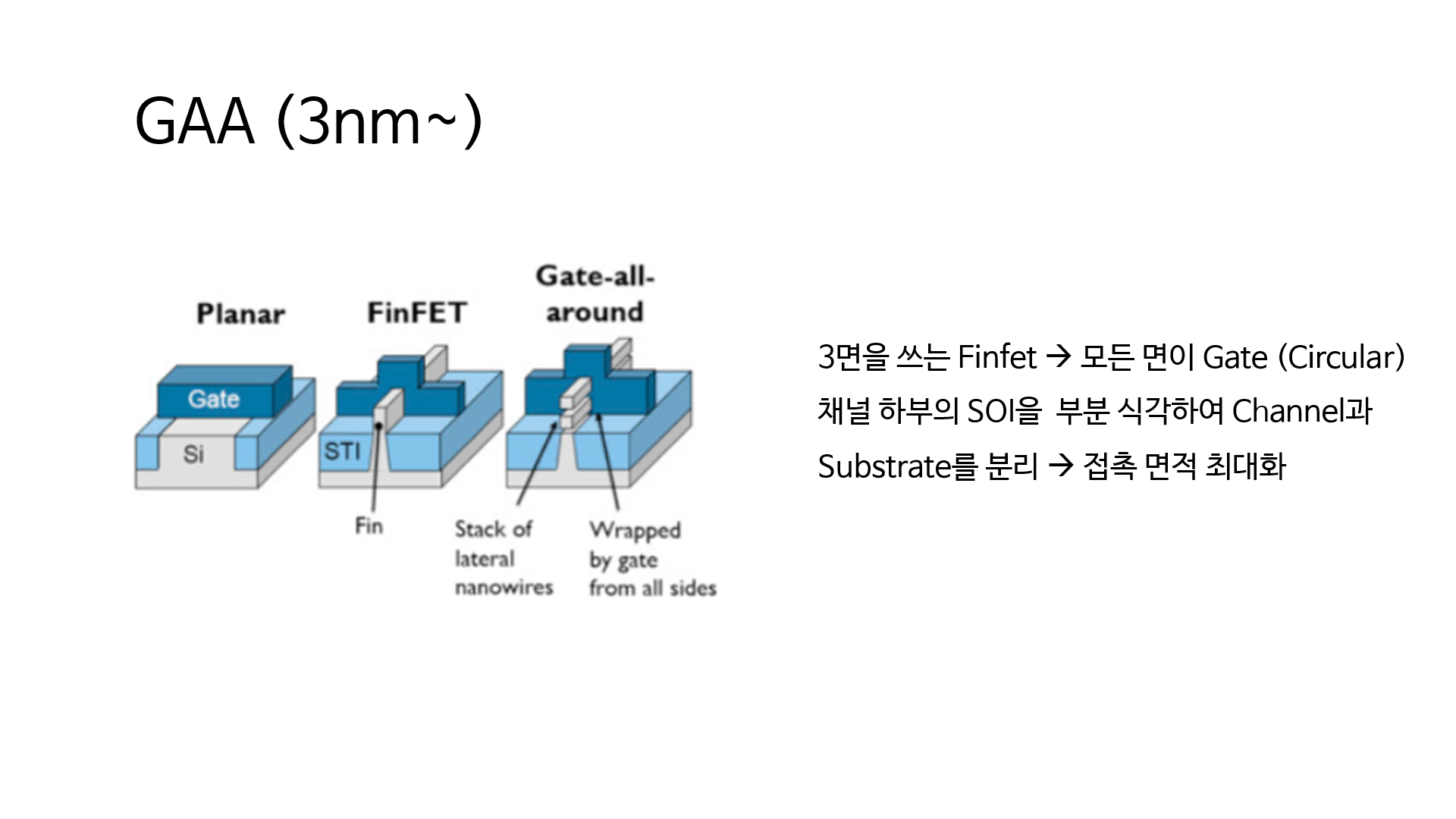
GAA is a three-sided FinFET with a circular gate on all sides and can be created by partially etching the SOI at the bottom of the channel to separate the channel and the substrate. Accordingly, the contact area may be maximized. It is a technology that will be used in nano processes of less than 3 nm in Samsung and TSMC.

With the roadmap of Samsung Foundry, it can be seen that the initial production of the 3nm GAAFet process will begin in 2020.