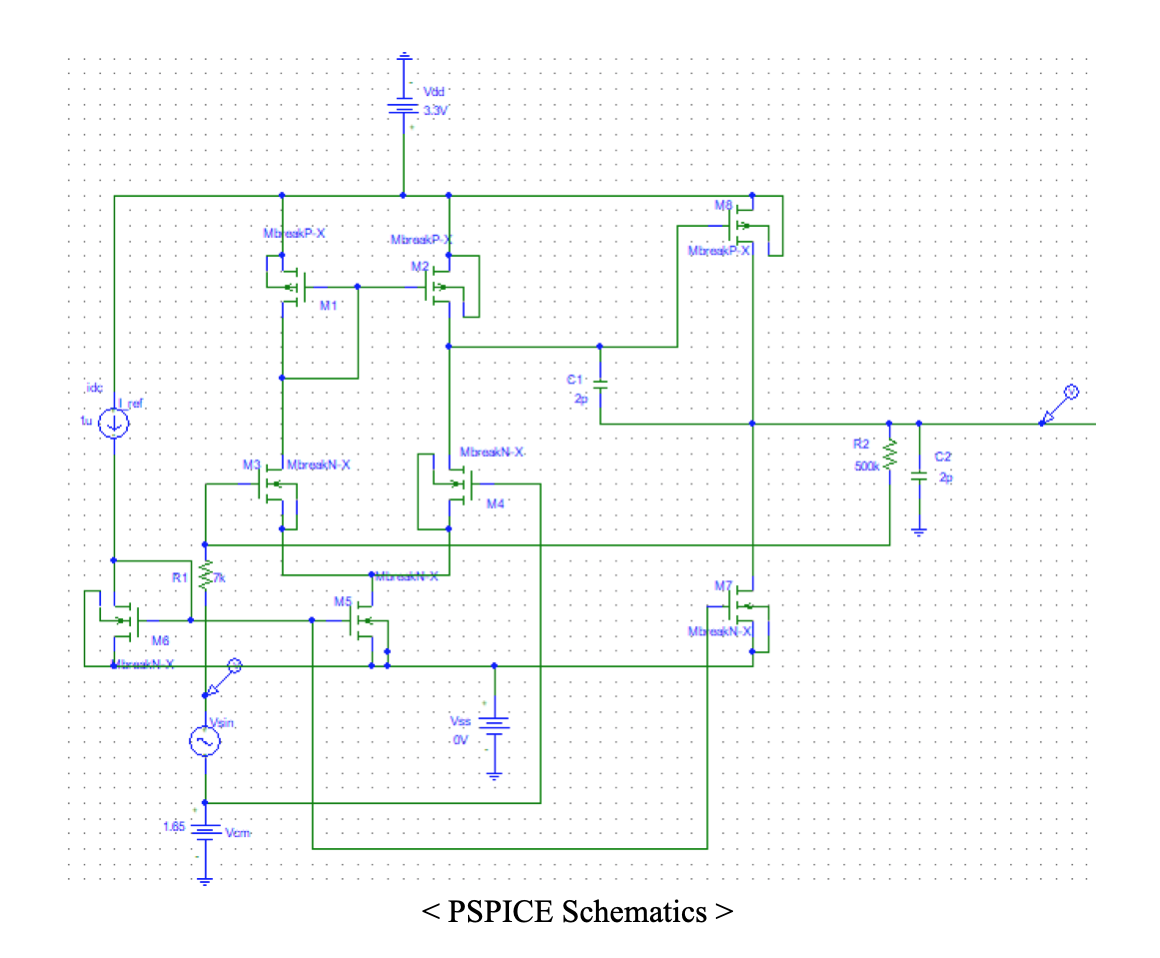
We designed the 2-stage CMOS Amplifier as above. When we design the amplifier, we should first set the differential amplifier (M1~M5) as input to reduce the common noise. In this design, we used the MOS differential pair with active load with single-ended output. By the current mirror action of the active load, the extra current (I_M1-I_M2) due to the input fluctuation flows to the load, creates amplified voltage. The M1 and M2 are the PMOS, and the M3~M5 are the NMOS. Since the NMOS has the better property on the amplifying and the PMOS has better property to offer the current load, we arranged the MOSFET as above. Especially, M5 acts as a tail-current sink, which helps the stable operation of the differential amplifier (improving CMRR).
Then, we should place the amplifying stage, such as the common-source (CS) stage or the MOS inverter (D-D connection). We used the CS stage to the second amplification stage since the CS stage is the most general amplifying stage between the 3 MOS topologies (CS, CG, and SF).
Now, the 2-stage amplifying stages are designed. To operate the amplifier, we should give bias to each stage. Hence, we used the current mirror to give bias to each stage. To make the I_ref as a golden current (current source which does not depend on the bias condition or temperature variation), we placed the DC current source above M6. By current mirror action, M5, M7 MOS current sources gives the exactly same reference current to the differential and inverter stage. Note that we should make the drain and the gate of M6 as a diode-connection to prevent the floating node. Then, we placed some coupling capacitors to obtain the AC-wise signal.
Until now, we finished designing the CMOS operational amplifier. Finally, we just make the inverting amplifier with the 7k and 500k resistors. Consequently, we can obtain an amplified signal. Let us see the simulation result for the verification of the specification of the designed circuit.


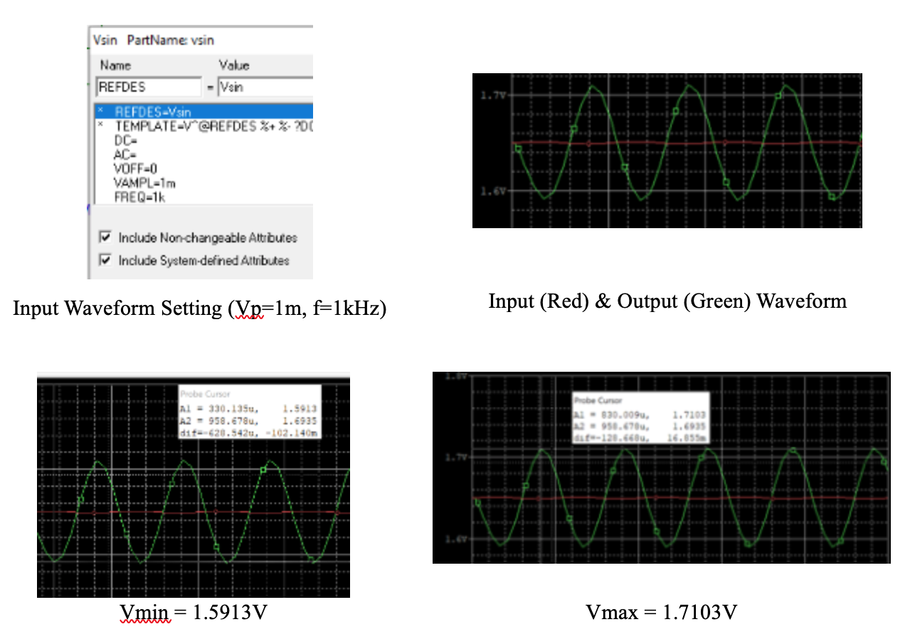
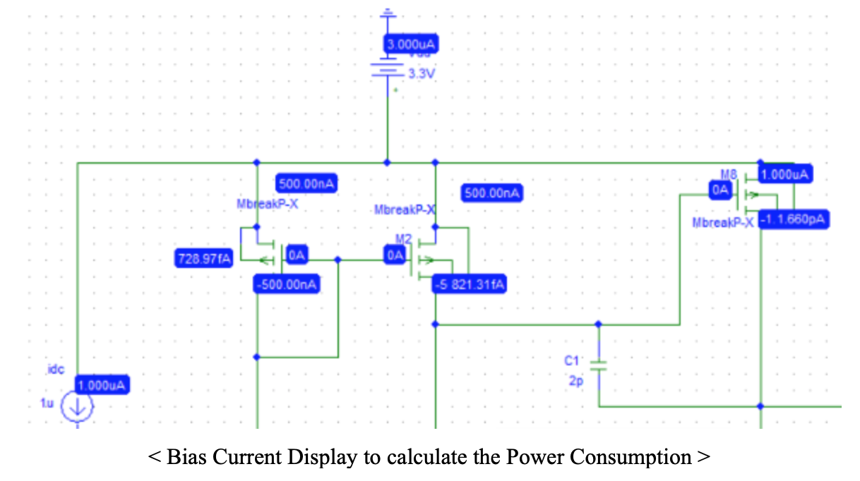
We verified the specifications of the designed circuit as above using PSPICE. The supply voltage V_DD and V_SS is equal to 3.3V and 0V respectively. We gave the 1mV amplitude with 1.65V common mode voltage and 1kHz frequency to the input voltage. The gain of the designed amplifier is 59.5, which is greater than 50. The peak-to-peak amplitude of the output voltage is 119mV, which is greater than 100mV. We calculated the power consumption as follows: P=VI=V_DDΣI_D=3.3V3μA = 0.0099mW, which is about 2 order lower than the 1mW power budget.
Let us investigate the similarities and differences compared to theoretical results. For the aspect of the power consumption, the theoretical and empirical values are exactly identical. The reason for this result came from the accuracy of the current mirror. As we can see the displayed current in the above figure, the current mirror exactly gives 1μA to each stage and divided to each transistor as we discussed in the theoretical analysis chapter.
However, the obtained gain is less than the theoretical value. The reason for this result may come from the assumption for calculating the gain. As we studied in the lecture, the precise gain is quite complicated compared to the intuitive gain analysis method, which we used to evaluate the theoretical values. This error may cause a gain difference. Also, the secondary effects such as the frequency response of devices, back bias effect, etc., were not considered when we evaluate the theoretical gain. If we consider those phenomena, we could evaluate the precise theoretical value which is close to the simulated gain. Nevertheless, if we think this error with the perspective of ‘10% error criteria’, which has been discussed frequently on our lecture, the error is about 9.8%, quite large but acceptable error.
[References]
[1] Behzad, Razavi. (2016). Design of Analog CMOS Integrated Circuits. : McGraw-Hill Education
[2] Suman, Shruti. (2019). Two Stage CMOS Operational Amplifier: Analysis and Design. SSRN Electronic Journal. 3. 40-44. 10.2139/ssrn.3433181.
[3] J. Mahattanakul. (2005), “Design procedure for two-stage CMOS operational amplifiers employing current buffer,” in IEEE Transactions on Circuits and Systems II: Express Briefs, vol. 52, no. 11, pp. 766-770, Nov. 2005, doi: 10.1109/TCSII.2005.852530.