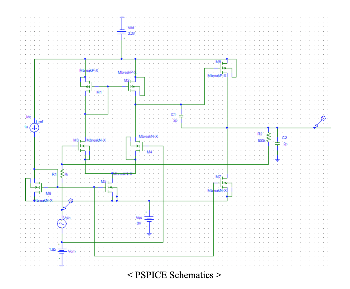
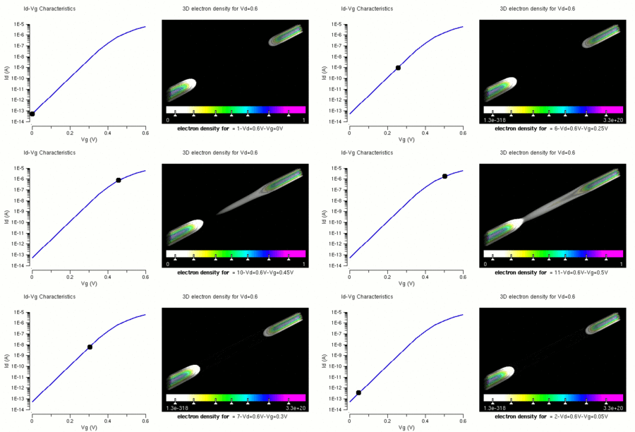
- Accelerating Semiconductor Design: AI Surrogate Modeling with PINO using NVIDIA PhysicsNeMo Framework
This project is ongoing, so stay tuned for updates!
Read More
Check out our Preprint: ArXiv Link: https://arxiv.org/abs/2603.06881
- From Theory to Tapeout: SAR-ADC Full-custom IC Design Project
The content is protected by a password to comply with NDA restrictions.
Read More
- LoRa/CSS: Overview, Demodulation and Decoding
Note: Source code details have been omitted for security reasons.
Read More
- GUI development with PyQT
PyQt is one of the most popular Python bindings for the Qt cross-platform C++ framework. Let us make a simple GUI to make a signal demodulator.
Read More
- AP Physics Tutoring Materials
Check out my AP Physics tutoring materials for high school students with a memorable class photo :)
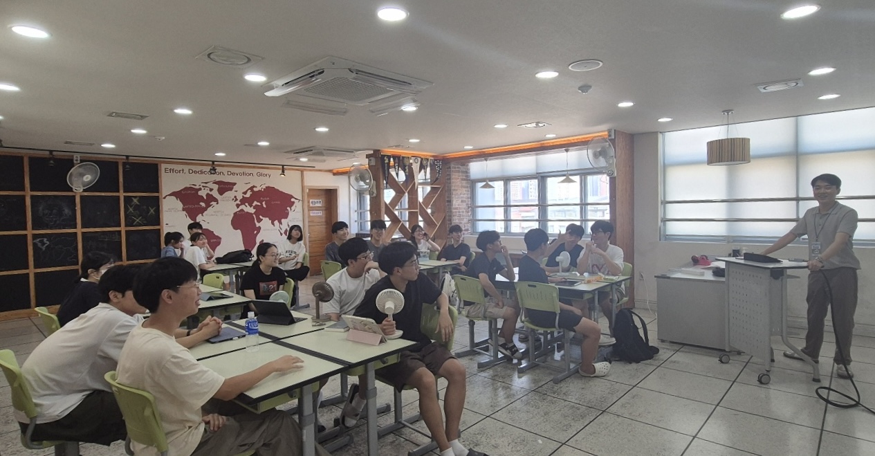
Read More
- Study Notes for Analog CMOS IC Design
Click to view the document if the browser does not support PDF Viewer.
Read More
- Analog Microelectronics Design
Click to view the document if the browser does not support PDF Viewer.
Read More
- Study Notes for RF Microelectronics
Click to view the document if the browser does not support PDF Viewer.
Read More
- Application on the Semiconductor Devices and Deposition Method
Project Description
Read More
Investigate the following topics on your material - ZrO2.
- An impression and final report for Samsung Electronics Internship

DSR Tower, Laboratory of Samsung Electronics 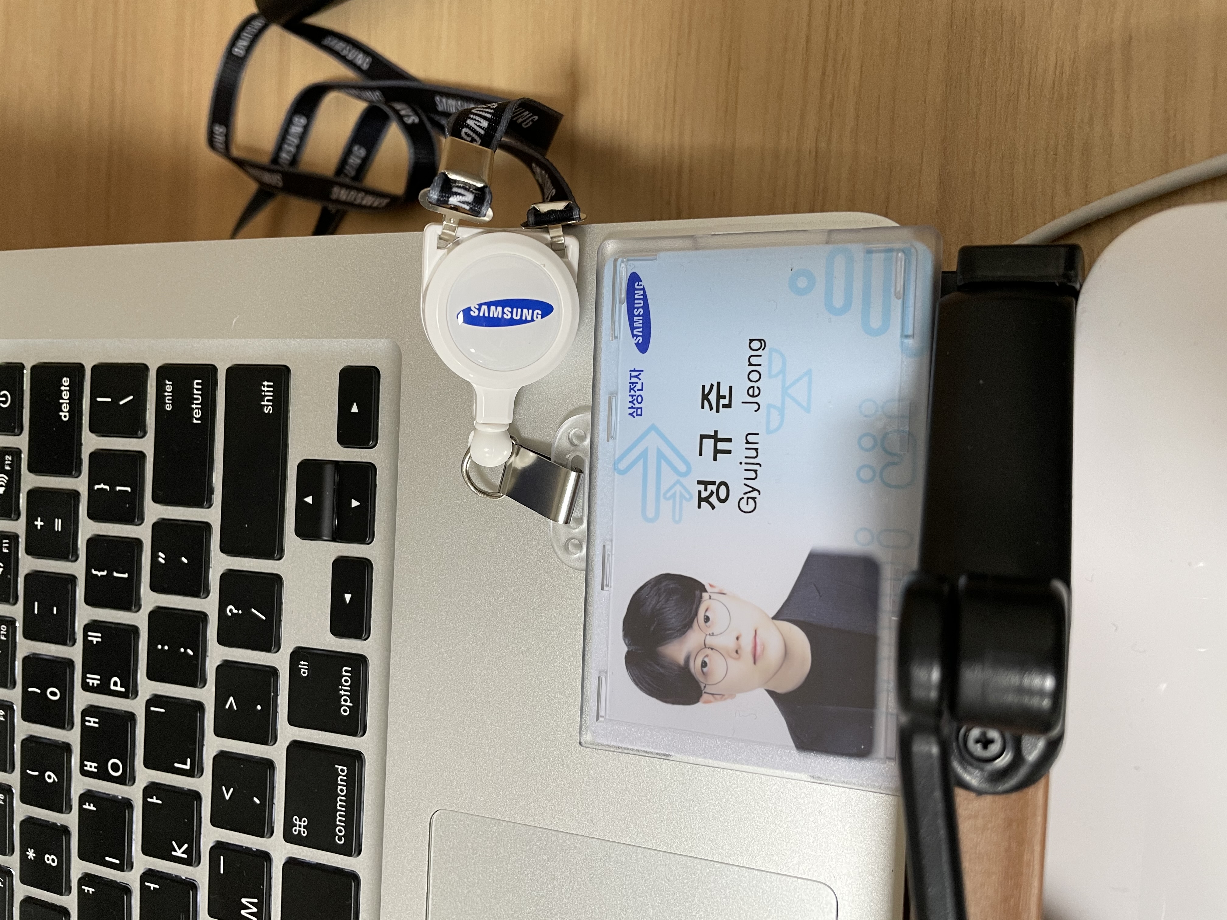
ID Card of Samsung Electronics Read More
- ISSCC Paper Review: THz Imager by Yokoyama(2019)
Click to view the document if the browser does not support PDF Viewer.
Read More
- PMC: Power Management IP on CIS utilizing Cyclic ADC
This project is conducted by studying various ADC architectures- SAR, Pipeline, and Cyclic ADCs- and investigating the principle of how Cyclic ADCs designed by applying them to PMC (Power Management IP). Subsequently, we designed the components of MDAC (Multiplying-DAC)- capacitance, amplifier, S&H, and reference. Finally, timing response/SNDR Simulation of MDAC and flash were conducted to understand the operating principles of PMC ADC and analyze the results to study the overall operating principles of PMC.
Read More
- TMC: Temperature Management on CIS using chopper
Note: The details cannot be disclosed here due to confidentiality concerns
Read More
- ABBG: Adaptive Body Bias Generator in CIS
In SoC, more and more Logic Gate is required according to Moore’s law, and accordingly, the power consumption also increases. The heat generated in highly integrated circuits resulted in the rise of the consideration element of operating temperature compared to the existing designed circuits. When the operating temperature is shaken, Vth changes according to the body effect, which may result in performance degradation. Therefore, when the temperature rises with the sensor that measures the temperature, the need for a feedback circuit that adjusts the body Bias has begun to emerge. The Adaptive Body Bias Generator (hereinafter referred to as ABBG) can be said to be a block that plays a role in adjusting the body Bias of each transistor more quickly and accurately according to the sensed temperature.
Read More
- JSSC Paper Study: Rail-to-Rail Op-Amp by Hogervost(1994)
Click to view the document if the browser does not support PDF Viewer.
Read More
- DBR: Doubler of CIS
In a CIS circuit, a Doubler is a block that produces a clear voltage of 4.5V, which is about twice as high as the nominal voltage of 2.5V. The most main component of this DBR Block is the charge pump. A charge pump (CP) is a circuit that uses the charge conservation law of a capacitor to generate a higher voltage than a power source. Using these charge pumps makes charge transfer easier on Pixel and can show better performance at the dark level or power immunity.
Read More
- ISSCC Paper Review: LiDAR Sensor using TDC/ADC hybrid SoC by Yoshioka(2018)
Click to view the document if the browser does not support PDF Viewer.
Read More
- EDA tools: Cadence Spectre and HSPICE
I learned how to handle various EDA tools such as Spectre of Cadence and HSPICE of Synopsys when I joined the company in the third week of March. The Analog IP team of Samsung Electronics’ LSI division conducted the Schematic and Layout with Cadence, and created Simulation Bench with HSPICE to conduct the simulation. In the laboratory, it took time to adapt because it was a process that was quite different from the ones that conducted both Schematics, Layout, and Simulation using Cadence Spectre. After creating Schematics in Cadence, Netlist is extracted, and then the HSPICE input bench is created using VIM Editor in a Linux working environment to create input waveforms, voltage, temperature, and type of analysis to be reported and run simulations.
Read More
- Unity Gain Buffer Design
Click to view the document if the browser does not support PDF Viewer.
Read More
- Cadence Virtuoso Manual
Cadence Virtuoso Manual
Read More
- Low Noise Electronics
- Coping with offset ~ Phase Locked Loop
Click to view the document if the browser does not support PDF Viewer.
- Coping with offset ~ Phase Locked Loop
- Modeling Periodic Jitter Sensor using Stochastic TDC without Reference Clock with Simulink
Click to view the document if the browser does not support PDF Viewer.
Read More
- ISSCC 2018 Paper: Period Jitter-Sensor Using Stochastic TDC
Click to view the document if the browser does not support PDF Viewer.
Read More
- Electronics Design Lab Compilation
Electronics Design Lab Compilation
Read More
Click to download!
- Issues and Solutions of the Modern Semiconductor IC Technology
Issues and Solutions of the Modern Semiconductor IC Technology
Read More
- Silvaco Simulation to minimize Bird’s Beak
Silvaco Simulation to acquire optimum condition to minimize Bird’s Beak
Read More
- Keynote for Microelectronics Project
Microelectronics Project Description: Total Score- A+ (1 of 80)
Freely select 3 of the concepts on the class slide and create a slide to present the concept.
The scoring criteria are as follows:- Are you explaining well what you introduced in class?
- Is the concept introduced in-depth? e.g., Additional points when an example with concept applied or a higher concept is introduced. If the concept introduced is more novel than others, you can get additional points. If you prove what you learned in class through experiments, you can additional points.
- Is the concept introduced to be logical?, e.g., If what is being described is correct and the flow is smooth, you can get additional points
- Whether the content of the produced slide is legible, e.g., clear picture, neat formula, clear explanation.
- Report for 2019 Winter Semester Individual Research
Advanced CMOS Technologies
Read More
- BSIM Models: Device Modeling
Read More
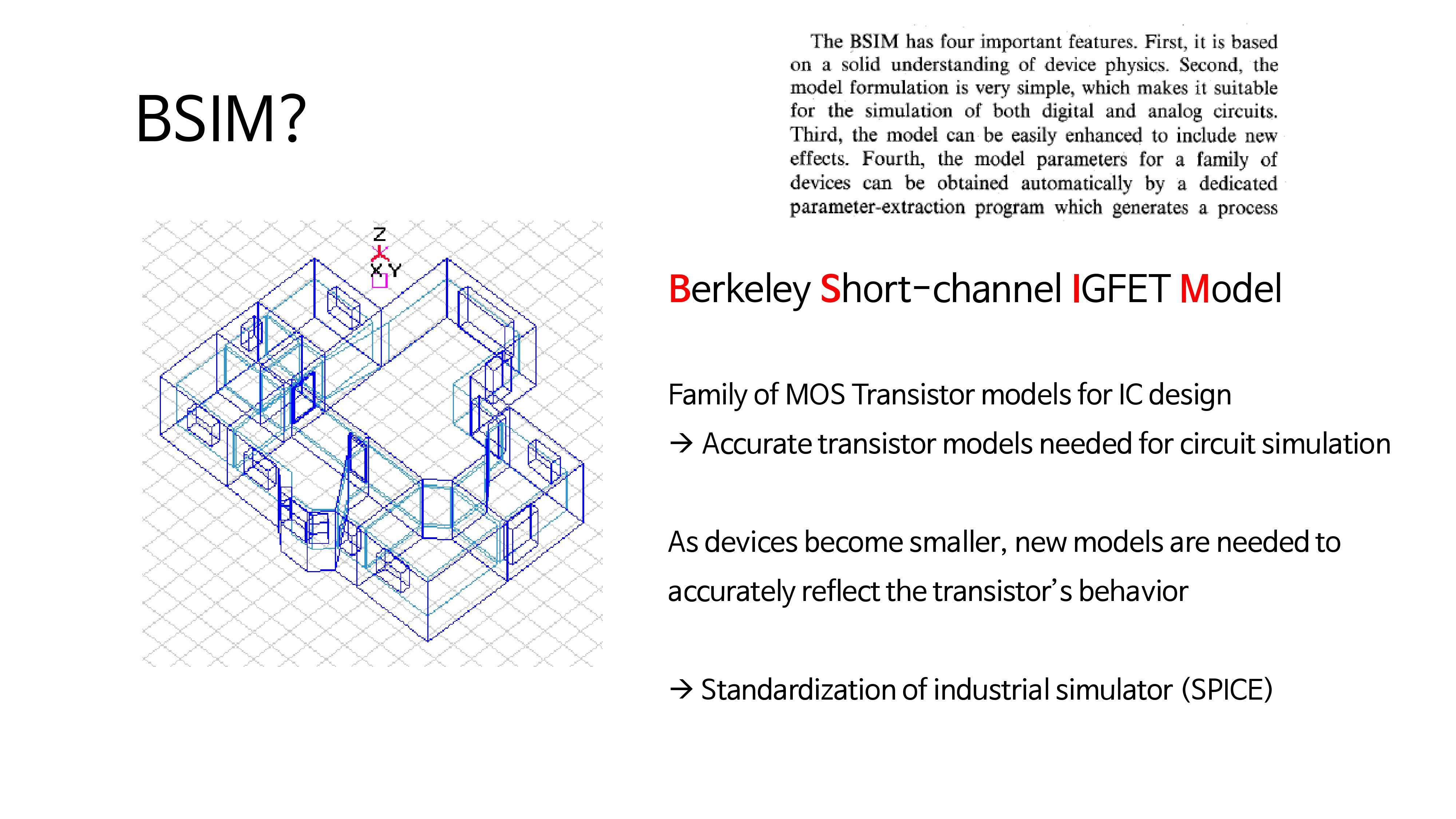 Computer simulation is necessary to make MOS devices. There should be a model required for these simulations. As the device became smaller, a new model was needed to reflect the behavior of the transistor. A model performing this role was produced by UC Berkeley. BSIM is an abbreviation for the Berkeley Short-channel IGFET (formerly known as MOSFET) model.
- Isolation Technique
Read More CMOS is an abbreviation for Complementary MOS, which is a MOS device with two different types of MOS elements placed in one wafer: n-channel MOS and p-channel MOS. When the two types of devices are placed on one substrate, various problems such as leakage current and latch-up occur. Today, let’s talk about isolation techniques that separate these elements.
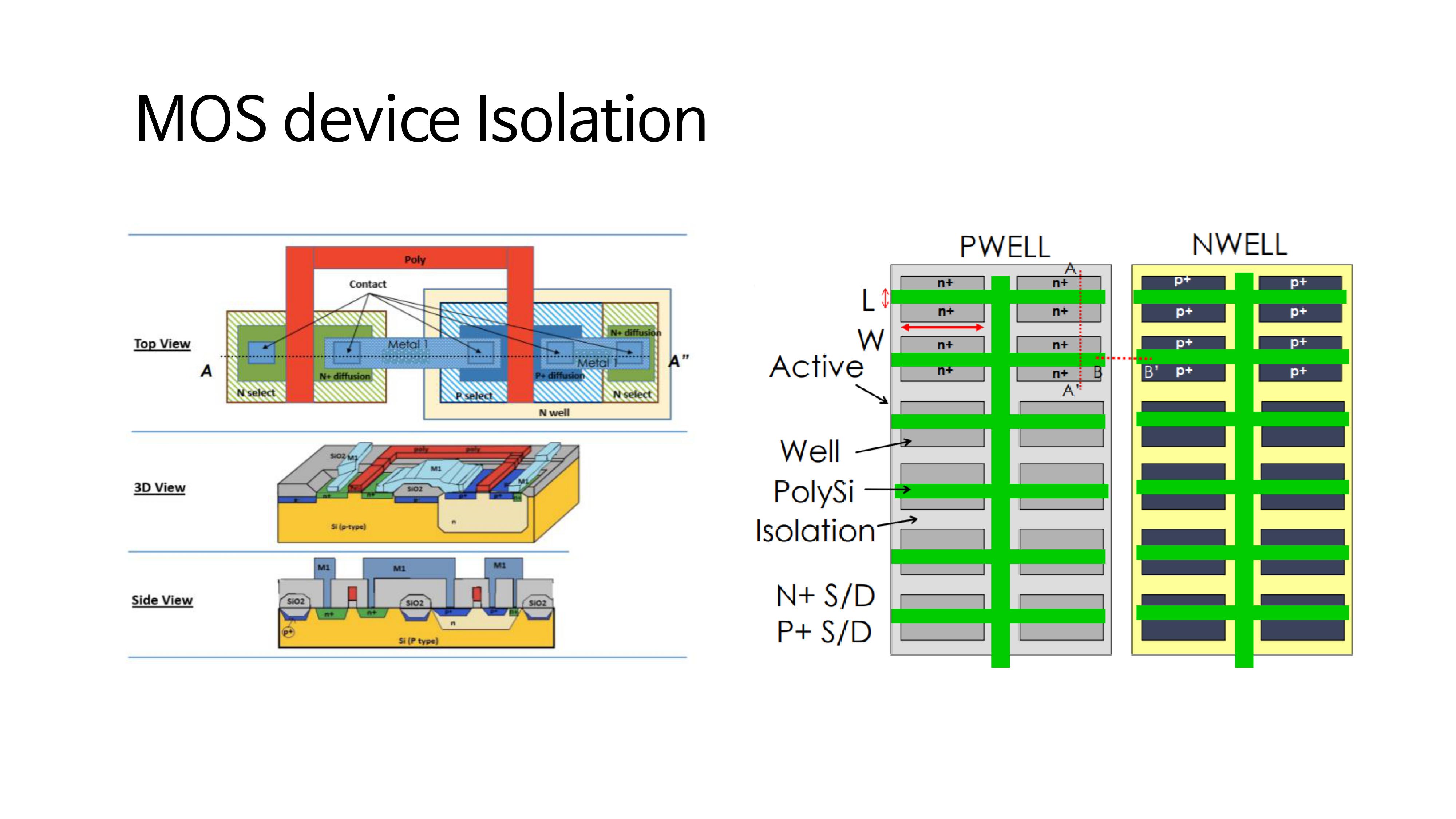
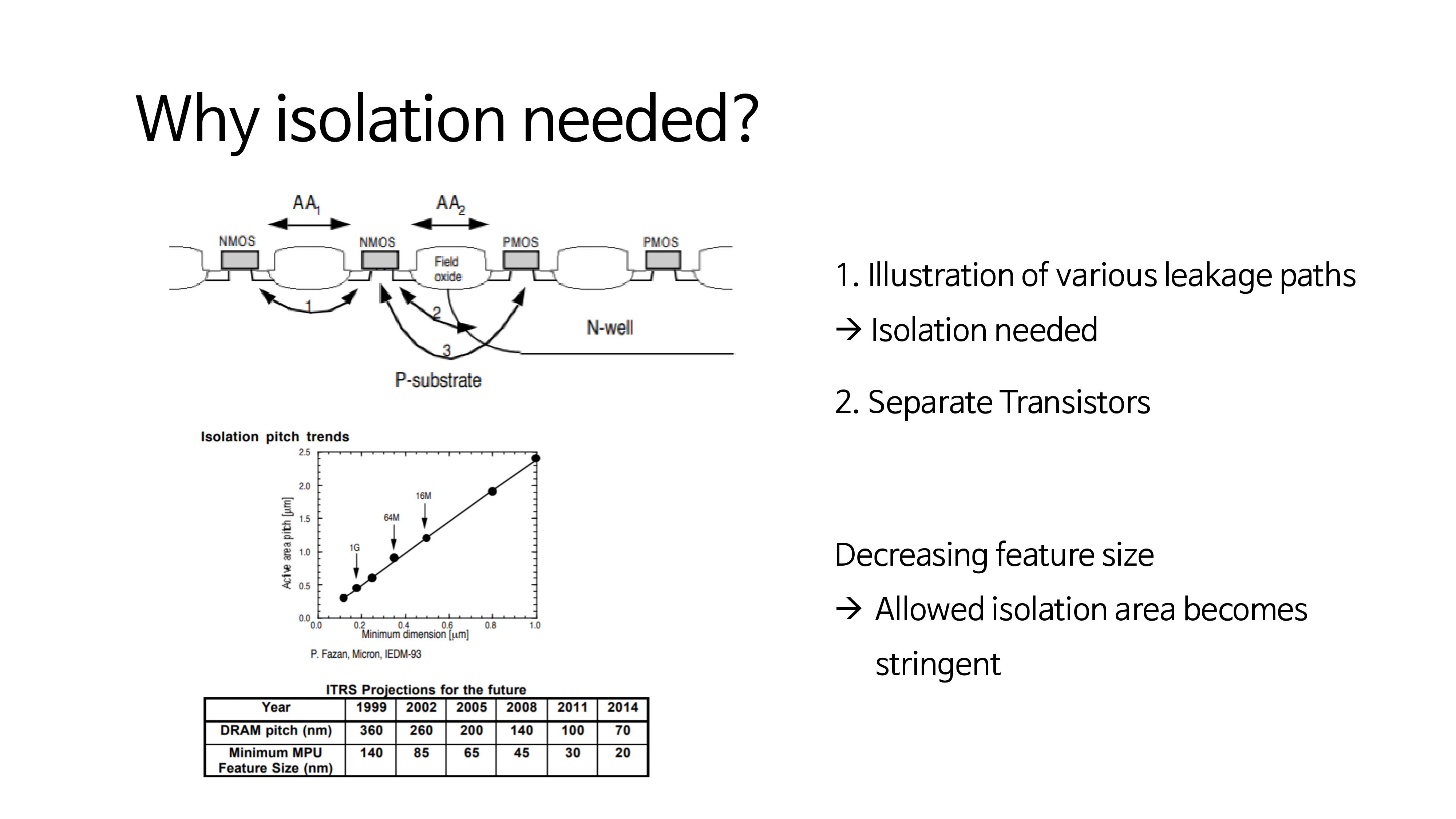 First, let’s find out why isolation is necessary. In the figure above, a leakage current path is illustrated, and isolation is required to prevent such a leakage current. Looking at the second figure, the space required for isolation is reduced while reducing the size of the device, so it can be seen that isolation also requires various technologies.
- Backend of IC process
Read More Semiconductors were manufactured through the semiconductor process introduced in the previous posting. However, semiconductors that are simply lumps of silicon do not perform their functions. Today, let’s look at the backend design, which is a subsequent process.
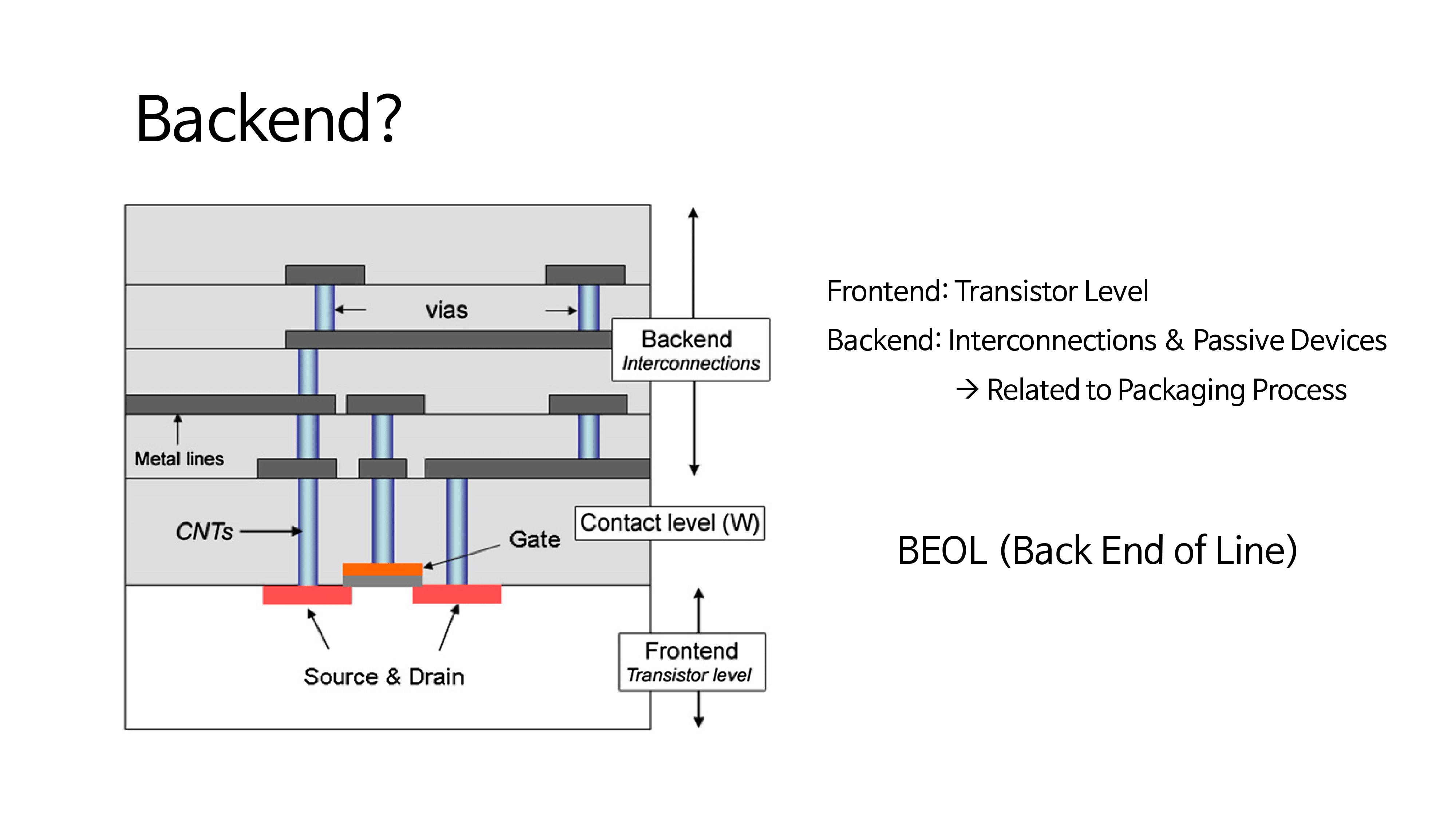 A frontend is a process at the Transistor level as in the previous posting method. A backend is a process of making chips with passive devices such as Interconnection or L or C.
- Scaling Trend of Semiconductor
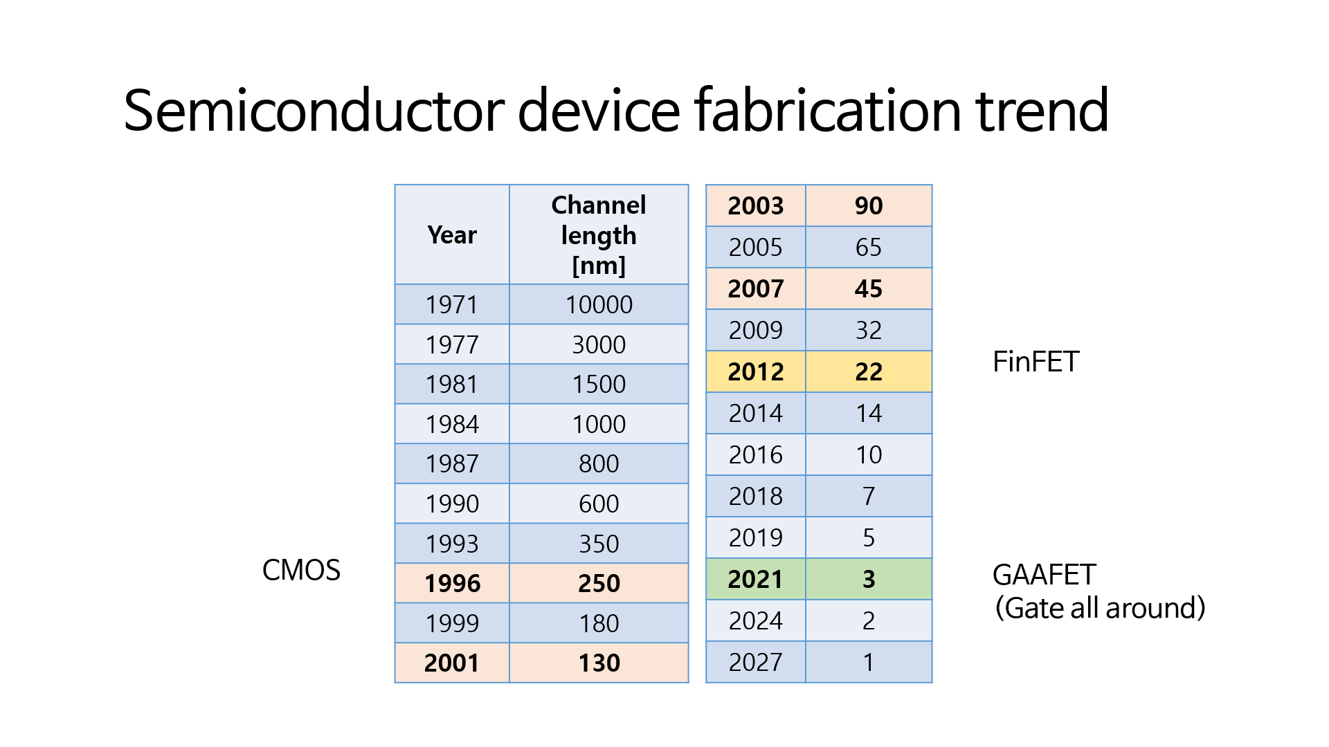
Read More Until last time, we learned why the device is made small and the Short Channel Effect that occurs when it is made small. It is important to make the device smaller in terms of yield and performance, but by making it smaller and smaller, abnormal characteristics begin to appear (SCE), and normal switching becomes impossible. Let’s take a look at the technology to overcome this Short Channel Effect.
- 3D FET Structure: FinFET and GAAFET
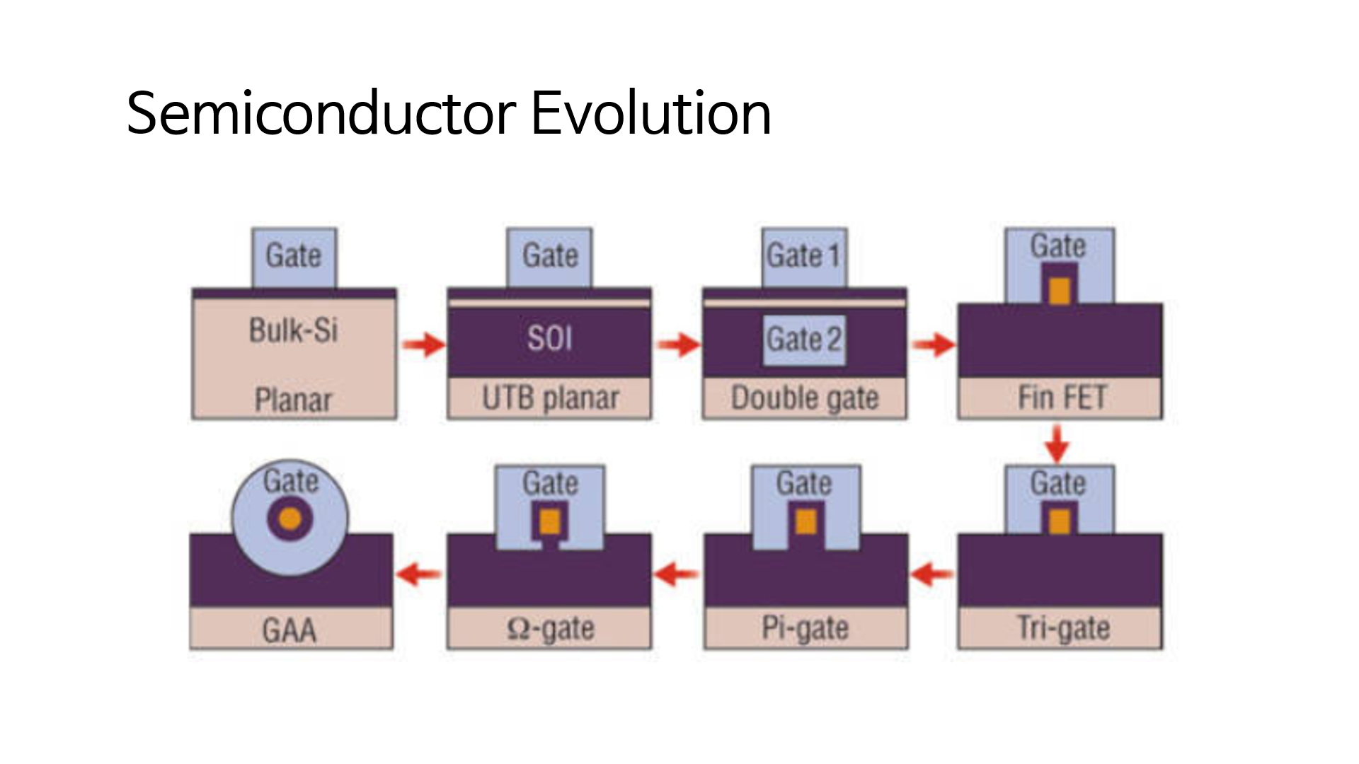
Smaller devices are needed to achieve faster and higher yields. However, due to various matters such as DIBL, punch-through, SS, and Hot Carrier Effect caused by Short Channel Effect, we need to find a way to solve this Short Channel Effect. Engineers attempted material changes in Planer MOS in a material science way, such as widening the gap between High-K and silicon lattice. However, there is a limit to this, so it was decided to change the shape of the FET altogether.
Read More
