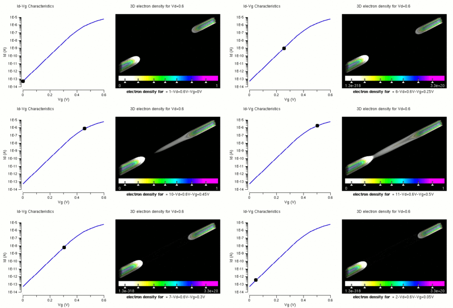
The semiconductor chip size is getting smaller and smaller. The cellphone on our hand shows overwhelming performance than the computer that is estimated as superlative about ten years ago. That huge computer is on our hand. This means the consumer requires more performance, but the footprint is limited.
Until today, engineers focused on minimizing the device’s size to enhance performance. Since engineers developed the 10um MOS in 1971, following Moore’s law, the up-to-date mass production chip size is about 7nm. The engineers in the front-end process try to solve this problem by modulating the structure of the device, such as FinFET or GAAFET to maximize the controllability of the gate voltage, and the back-end process engineers try to solve the problem by modulating packaging methods, such as FOWLP or FOPLP.
However, with nowadays technologies, we are in trouble to improve the silicon semiconductor’s performance dramatically due to the physical limit. Since the channel length approaches to the atomic size, quantum mechanical problems come to the fore. Although it may be possible, still challenging. The development of alternative transistor architectures, rather than MOSFET, is urgently needed.
There are two main roles of the semiconductor device: amplification and switching of the signal. Namely, a good device should give the signal when we want and amplify the signal. One interesting thing is that in the past years, engineers focused on making more higher current with semiconductors, but nowadays, engineers focusing on the speed to reach the highest current. The indicator of the response speed to peak current called ‘Subthreshold Swing (SS)’. The lower SS means the device has a fast response speed. However, nowadays mass-production devices cannot break-through the 60mV/dec, the physical limit of SS in room temperature.


Engineers thought that if we use this phenomenon, we can solve the problem to overcome the limit of SS and make a faster device. We can think if we can penetrate the barrier without the additional force, it means that we can obtain the fast response of the device, which means lower SS. This device is called ‘TFET (Tunnel Field Effect Transistor)’. Engineers succeeded to make SS below the 60mV/dec. That is, we can switch the device much faster.

Another matter of the TFET is QCE(Quantum Confinement Effect), which is the concept we studied. For short, if the crystal size decreases, the bandgap size increases. This increased bandgap degrades the current characteristics that make ON-state current worse. This effect could be explained by the quantum dot effect- bandgap increases so wavelength decreases, shows blue-shift. 
Also, TFET’s current is much smaller than the normal FET device. The reasons for this kind of phenomena are that TFET use carriers in the valence band of p-type. Unlike MOSFET- source and drain types are the same as n-type in n-MOS case, TFET has a p-type source, and the electron comes from a p-type source. By the Mass-Action law of semiconductor, the electron number in p-type is much less than the n-type source. 
These shortages made TFET less practical device than MOSFET, and these off-state problems should be solved. Now, we will obtain the improvement of the performance of TFET.
Before we see the improvement method in-depth, let’s review the bandgap concept. If the bandgap is too large, carriers cannot move so that the current cannot flow, known as an insulator. If the bandgap is too small, carriers can move freely that the current flow enormously, called metal (conductor). However, as we have seen before, the object of the semiconductor device is the switching and amplifying, and these could be done by manipulating the energy bandgap between CB and VB. For instance, if we connect the boron-implanted silicon(p-type) and phosphorus-implanted silicon(n-type), by the energy band level difference, we can control the current flow, known as a p-n junction. 
The bandgap engineering has been researched to improve the performance of TFET. The key of the performance is to make TFET enhance tunneling on on-state, but prevent tunneling on off-state. We can improve the properties of current of TFET with manipulating bandgap with different materials.


With black phosphorus, we can give different bandgap on the same material. If we vary the number of layers, we can manipulate the bandgap. Namely, we can obtain different bandgap by giving the black phosphorus thickness difference without connecting the different materials. This device shows 23-24mV/dec SS, significant reduction compared to the previous device- 60mV/dec. 
In conclusion, TFET with the black phosphorus gives us much improved SS, i.e., improved responsibility of the device without the defect on the boundary. With this device, we can make the super-fast and expeditious electronic devices that could be used in the next-generation.
[ References ]
[1] Fulay, P. P., & Lee, J.-K. (n.d.). Electronic, magnetic, and optical materials. Boca Raton: CRC press.
[2] Neamen, D. A. (2012). Semiconductor physics and devices. New York: McGraw-Hill.
[3] Seungho Kim et al, “Thickness-controlled black phosphorus tunnel field-effect transistor for low-power switches”, nature nanotechnology, 2020 (doi: 10.1038/s41565-019-0623-7)
[4] Tunnel field-effect transistor. (2020, April 7). Retrieved from: https://en.wikipedia.org/wiki/Tunnel_field-effect_transistor
[5] IT Learning. (2018, November 12). [Semiconductor Devices] TFET Bandgap Engineering. Retrieved from https://it-learning.tistory.com/15