 Until last time, we learned why the device is made small and the Short Channel Effect that occurs when it is made small. It is important to make the device smaller in terms of yield and performance, but by making it smaller and smaller, abnormal characteristics begin to appear (SCE), and normal switching becomes impossible. Let’s take a look at the technology to overcome this Short Channel Effect.

After Dr. Kang Dae-won’s development of MOSFET transistors in 1971, the semiconductor industry, which started with a channel length of 10 micrometers, will now be developed by leading companies such as Samsung, Hynix, and TSMC in 2019. In December 2019, Intel, a global semiconductor company, unveiled a roadmap aimed at developing a 1nm process by 2027 at a technology conference. Today, let’s look at the technologies that went into the 250, 130, 90, and 45 nano processes which is marked in red.

Before looking at each nano process, there is the most well-known law in the semiconductor industry. It is Moore’s law proposed by Gordon Moore, co-founder of Intel, a global semiconductor company. This is the law that the performance of semiconductor integrated circuits doubles every 24 months. In other words, it can be thought that the performance is doubled every two years.
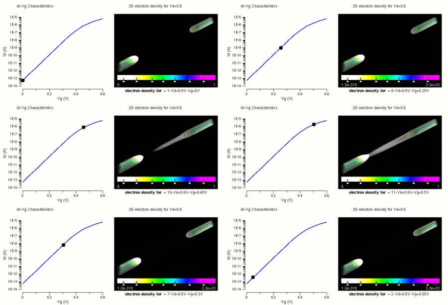
However, it is gradually beginning to reach the limits of scaling. If the channel length is reduced as shown in the second picture, tunneling occurs as shown in the right picture, and a phenomenon in which the device no longer functions properly occurs. Even if it is possible, there is an opinion that it should be given up due to the problem of cost. There are different opinions that Moore’s law is no longer valid and still valid.
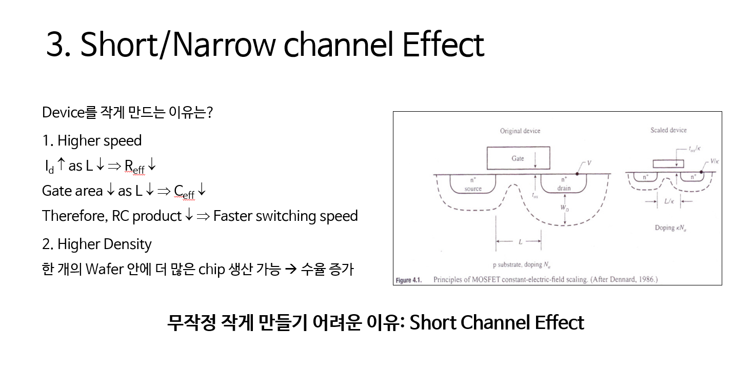
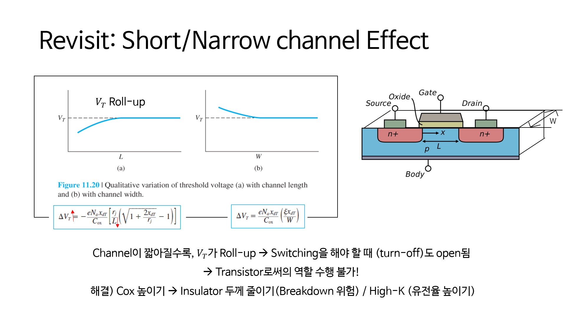
It’s the Short Channel Effect that we saw last time. It is important to make the device smaller in terms of yield and performance, but the channel is shortened by making it smaller, which causes the Threshold Voltage to roll up, and results in being opened when switching is required, which cannot function as a transistor. Now let’s find out how we overcame the Short Channel Effect for each nano process.
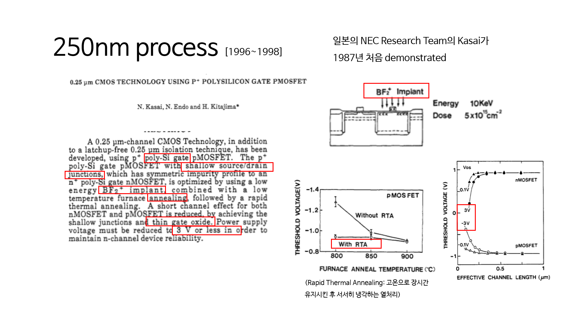
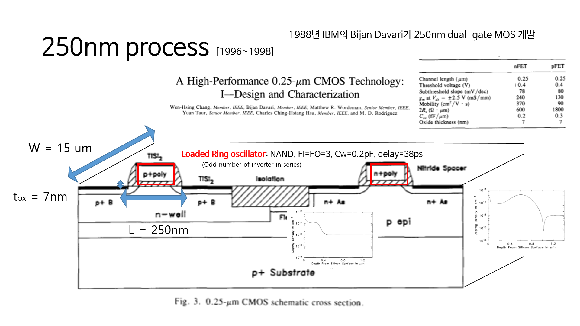
The 250 nm process was first commercialized in 1996, and in 1987, an engineer named Kasai of the NEC Research Team in Japan succeeded in demostrate. Kasai overcame the Short Channel Effect through the following method.
- poly-Si Gate
- Shallow S/D junctions
- BF2+ implant
- RTA (Rapid Thermal Annealing)
- Thin Gate oxide (refer to Vt roll up formula)
Looking at the graph of the paper, it may be seen that the RTA, that is, the annealing of rapidly cooling after being maintained at a high temperature for a long time, has significantly decreased in V roll-up compared to not being performed.
IBM’s Bijan Davari published the structure of the 250 nm dual-gate CMOS in his paper. The structure of the element is shown in the second figure.
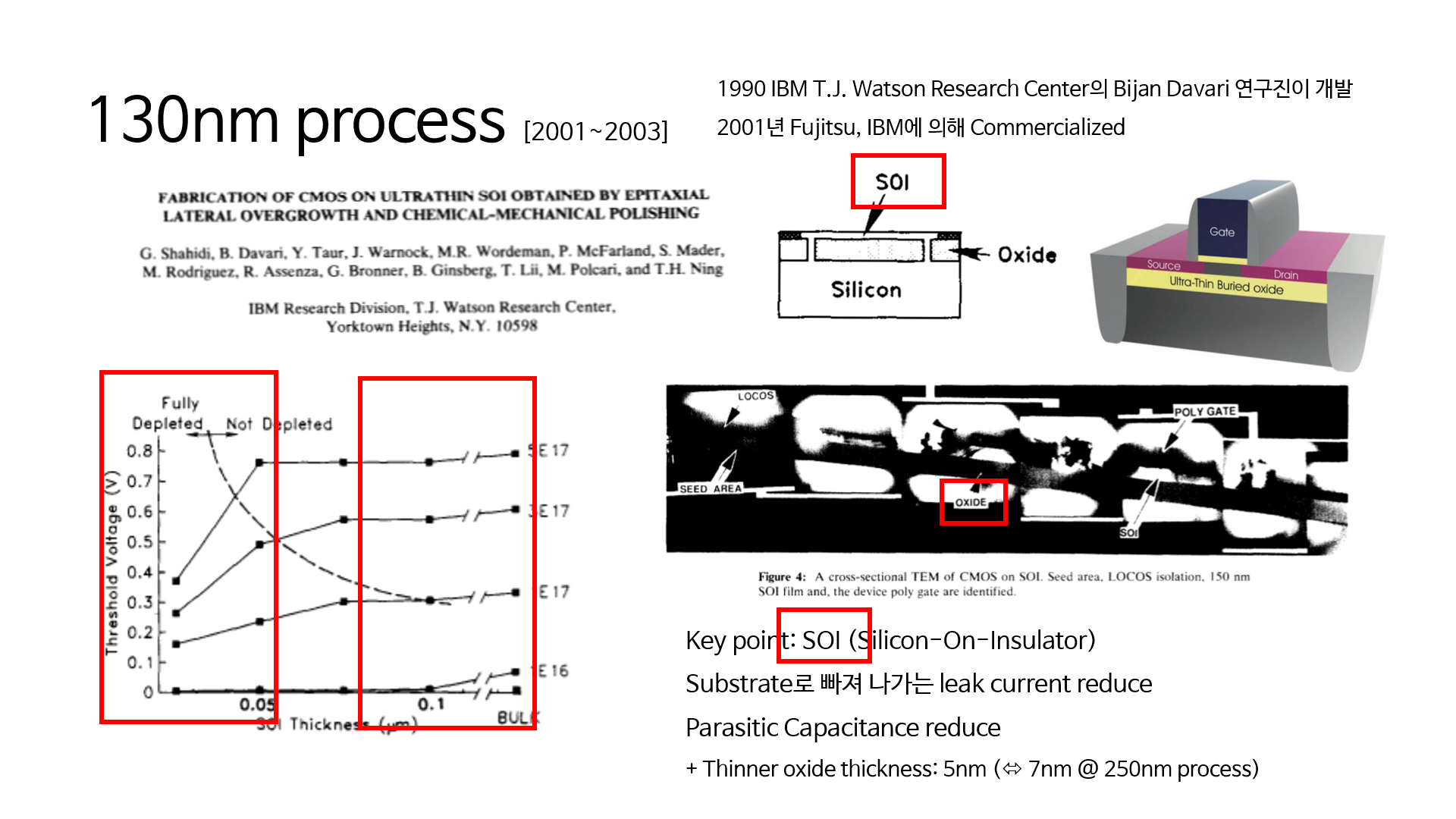
The 130 nm process was commercialized in 2001 by companies such as Fujitsu and IBM, and was developed by Bijan Davari at IBM’s T.J. Watson Research Center in 1990. The key points in this process are SOI, or silicon-on-insulator technique. Through this method, the leakage current exiting the substrate could be reduced, and the parasitic storage capacity could be drastically reduced. It was also possible to solve the latch-up problem recognized in MOS devices. Other factors used a thinner oxide thickness (7 nm->5 nm) than in the 250 nm process.
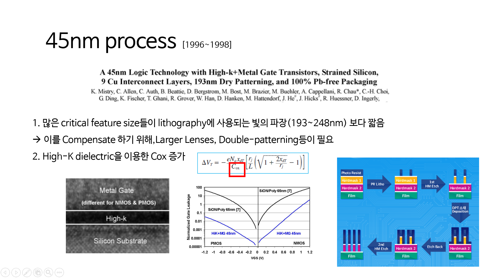
From the 45nm process, there are many problems, and first, there is a problem that the feature size of the device is smaller than 193nm, which is the wavelength of light used in the photo process called lithography. To compensate for this, a more precise photolithography process could be created through larger lenses and double-patterning.
In addition, to increase Cox in the Vt roll-up formula, the oxide layer, which was too thin, resulted in an undesirable effect such as tunneling, using a high-K dielectric constant (K) to compensate for it.