Accelerating TCAD: AI Surrogate Modeling with PINO using NVIDIA PhysicsNeMo Framework
Tutorial Video
Paper (ICMC 2026): Physics-informed AI Accelerated Retention Analysis of Ferroelectric Vertical NAND: From Day-Scale TCAD to Second-Scale Surrogate Model (arXiv:2603.06881)
Demo Code: github.com/gyulab/PINO-for-Semiconductor
Tutorial Slides: AI-Surrogate-modeling-tutorial.pdf
This work is a collaboration between Georgia Tech, Samsung Electronics, and NVIDIA, and was presented at ICMC (International Compact Modeling Conference) 2026!
Note) We are preparing for the journal extension, stay tuned for updates!
Motivation: TCAD Bottleneck for Fe-VNAND Retention Analysis
Ferroelectric FET (FeFET)-based vertical NAND (Fe-VNAND) is a promising candidate to overcome the Z-scaling limitations of 3D NAND with lower programming voltages. However, its data retention is hindered by a complex, time-dependent interplay between ferroelectric depolarization and charge detrapping at the dielectric interfaces. Optimizing the gate stack against these effects requires exploring a huge design space—geometry, temperature, and retention time.
Conventional Technology Computer-Aided Design (TCAD) is accurate but computationally prohibitive: a single rigorous simulation sweeping temperature and time can take over 24 hours, and the cost scales linearly with every additional variable. To solve this, we developed a Physics-Informed Neural Operator (PINO)-based AI surrogate model on the NVIDIA PhysicsNeMo framework that predicts 2D physics maps, ID-VG curves, and Vth retention loss with near-TCAD accuracy in seconds.
Device and TCAD Training Data
We study a single FeFET with an interlayer-engineered gate stack, where a Tunnel Dielectric Layer (TDL) is inserted between ferroelectric layers (HZO/TDL/HZO). During erase, charges accumulate at the HZO/TDL interface via Fowler-Nordheim tunneling and counteract the depolarization field. During retention, these screening charges detrap, which exacerbates the depolarization field and accelerates polarization loss.
Training data were generated with Synopsys Sentaurus TCAD (ferroelectric Preisach model + FN tunneling, retention up to 104 s) by sweeping three inputs, giving only 120 TCAD sweeps in total:
| Input Sweep Parameter | Values |
|---|---|
| HZO Thickness | {5, 6, 7, 8, 9} nm |
| Temperature | {300, 358, 400, 473} K |
| Retention Time | {0, 1e0, 1e1, 1e2, 1e3, 1e4} s |
For each condition, we extract the ID-VG curve and internal 2D physics maps: electrostatic potential, polarization, and trapped electron/hole densities from the gate stack (HZO/TDL/HZO), and the current density from the entire device to capture channel conductance changes.
Methodology: Physics-Informed Neural Operator (PINO)
Our model is not a “black box.” Instead of directly mapping scalar inputs to ID-VG curves, it first predicts intermediate physics maps, which makes the surrogate a physically interpretable digital twin and acts as a physical regularizer for the downstream readout.
Architecture

The pipeline consists of three phases:
- Phase 1 – Input Embedding: Scalar device inputs (tHZO, T, log(τ)) are embedded into an input tensor.
- Phase 2 – PINO Physics Surrogate: A Fourier Neural Operator (FNO) backbone performs global convolutions in the Fourier domain and maps the inputs to resolution-invariant 2D physics fields (J, Qe,h, V, P) on a 256×256 grid. To avoid overfitting the sparse dataset, the FNO is strictly regularized: 4 Fourier layers, modes = 12, latent width = 32.
- Phase 3 – IV-Net Readout: A shallow CNN map encoder extracts features from the physics maps, while the original scalar inputs bypass the surrogate through a parallel MLP (scalar context injection). The two are fused to predict the final ID-VG curve. This residual path preserves global thermodynamic context (e.g., bake temperature) that cannot be extracted from purely electrostatic 2D maps.
Physics-Informed Loss Function
The key difference between a purely data-driven FNO and a PINO is the dual-loss objective:
where \(\mathcal{L}_{data}\) is the L2 error against TCAD ground truth, and \(\mathcal{L}_{physics}\) consists of two components:
- Poisson Residual: enforces that the predicted potential \(\phi\), charge density \(\rho\), and ferroelectric polarization \(P\) obey electrostatics.
- Monotonicity Constraint: enforces the monotonic decay of remnant polarization and trapped charge over retention time, penalizing unphysical glitches or oscillations.
This physics-informed loss constrains the hypothesis space when training data are sparse, which is exactly the regime of expensive semiconductor simulations.
Results
1. Reconstruction Accuracy of 2D Physics Maps
Validated against TCAD, the trained PINO reconstructs 2D profiles of electrostatic potential, trapped charge, and current density with a relative error of ~0.1%.


2. ID-VG Prediction and Retention Analysis
- Vth Accuracy: R2 > 0.998 for Vth (at ID = 100 nA) over all 120 sweep conditions.
- Unseen Temperature: The model produces physically consistent ΔVth retention curves at an unseen 350 K, lying between the 300 K and 400 K TCAD baselines.
- Physics vs. Data-Driven: The purely data-driven FNO overfits the sparse dataset and shows unstable ripples across the transfer curve, while the PINO predicts a smooth ID-VG response, improving RMSE by > 40% (0.080 → 0.047).
3. Computational Efficiency
| Metric | TCAD | AI Surrogate |
|---|---|---|
| Single sweep | 30 min | ~0.1 s (real-time) |
| Full sweep | 60 hrs | ~10 s |
| DSE coverage | Discrete (prone to blind spots) | Continuous (mesh-free interpolation) |
| Cost of optimization | Prohibitive | Minimal |
(TCAD: Intel Xeon Platinum 8470N 52-core CPU, AI surrogate: NVIDIA Titan RTX 24 GB GPU)
A full retention sweep goes from 60 hours to ~10 seconds, a speedup of four orders of magnitude (> 10,000×).
Open-Source Demo: PINO for Semiconductor
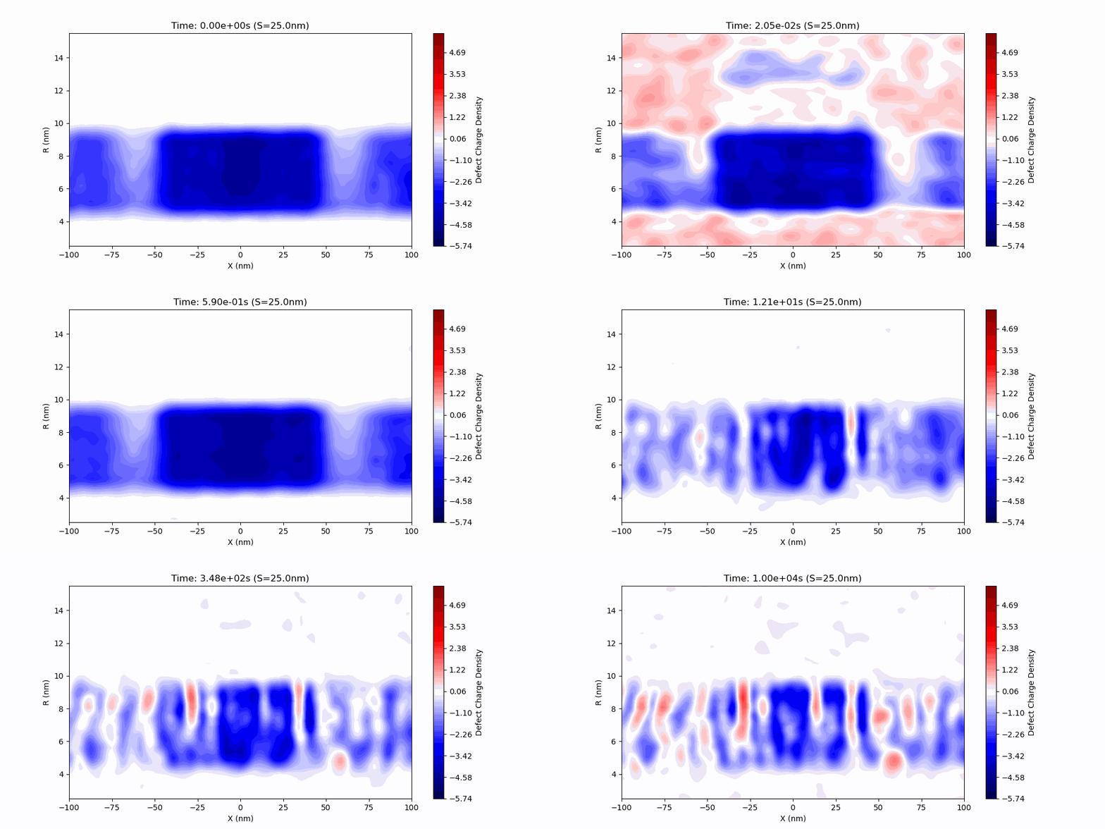
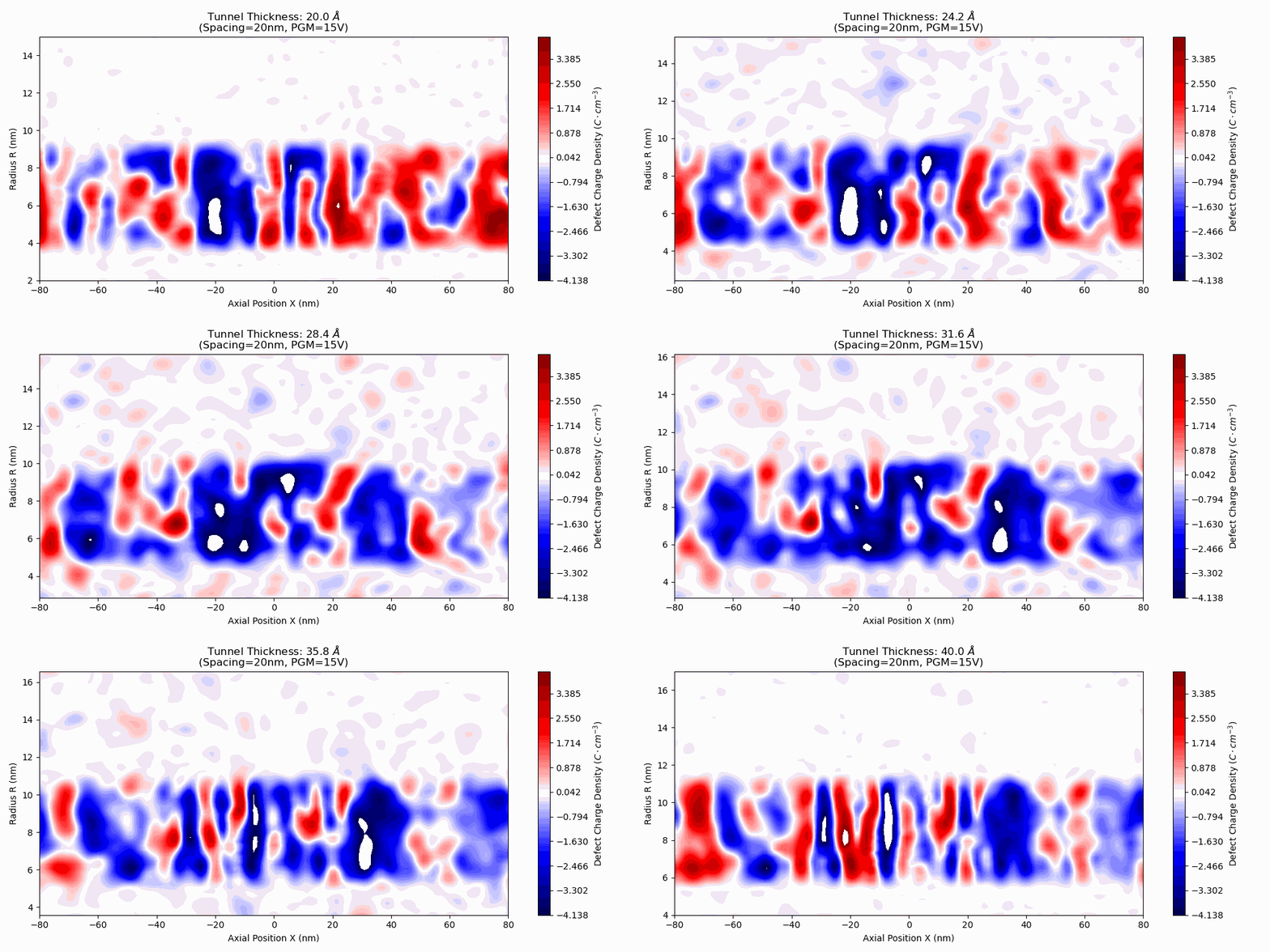
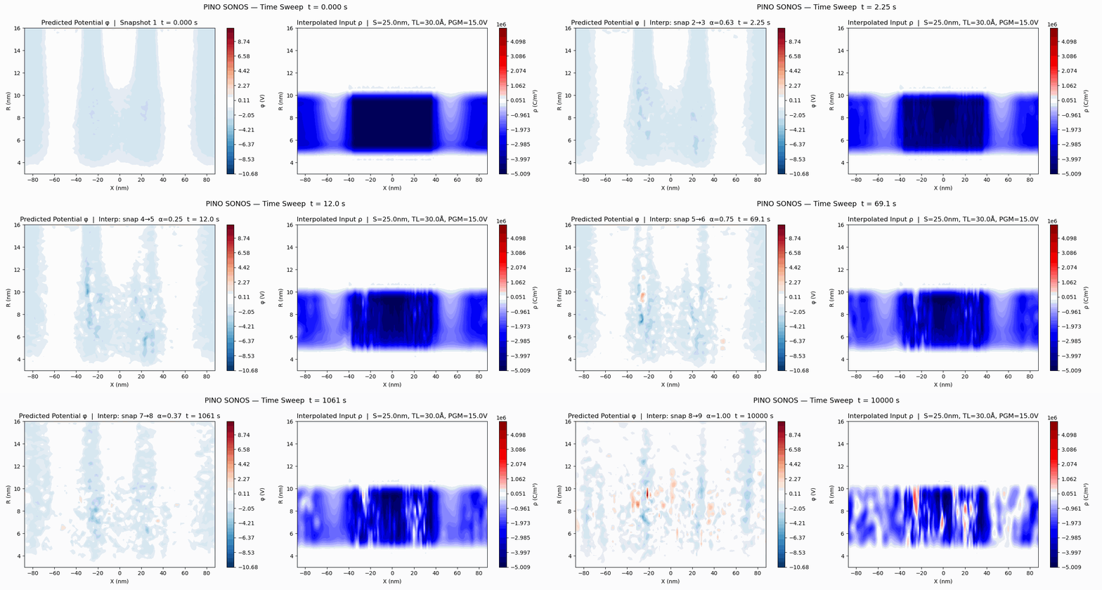
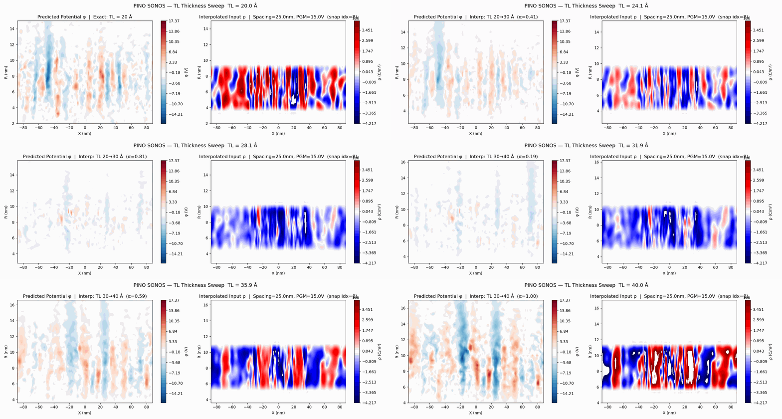
To make the workflow reproducible, we released a demo repository, PINO-for-Semiconductor, that applies the same NVIDIA PhysicsNeMo-based FNO/PINO pipeline to 3D SONOS NAND flash devices. Watch the tutorial video at the top of this post for a walkthrough.
PINO-for-Semiconductor/
├── code/
│   ├── train_fno_model_sonos.py    # Standard FNO, MSE loss (data-driven only)
│   ├── train_pino_model_sonos.py   # PINO with Poisson residual loss
│   ├── inference_time_sweep.py     # Time-evolution animation of defect charge density
│   └── inference_pino_time.py      # PINO time-sweep inference
├── docs/
│   └── AI-Surrogate-modeling-tutorial.pdf
└── results/                        # FNO vs. PINO visualizations (below)
In train_pino_model_sonos.py, the Poisson equation \(\varepsilon \nabla^2 \phi + \rho = 0\) is implemented as a custom PhysicsNeMo Node, and its residual is driven to zero alongside the data loss. The training data (AMAT Ginestra simulations) are not included due to EULA/NDA restrictions.
FNO (Data-Driven): Defect Charge Density
PINO (Physics-Informed): Predicted Potential from Charge Density
Preliminary Proof-of-Concept
Before the ICMC paper, we explored the framework on other configurations.
Design Space Exploration (Interpolation): Trained on 5, 7, and 9 nm HZO thicknesses, the model was queried for an unseen 8 nm device and predicted a max E-field of ~8.4 MV/cm, matching the verification TCAD simulation (30 min in TCAD vs. < 1 ms in AI).

AOS Channel String Array FeNAND: On a string array with amorphous oxide semiconductor (AOS) channels and Source/Gate/Drain regions, the AI reconstructed 2D current density maps with <1% reconstruction error, showing the model can handle complex boundaries and material interfaces needed for array-level modeling.


Summary and Future Work
We developed a physics-informed AI surrogate model that faithfully accelerates Fe-VNAND retention analysis:
- Efficiency: Trained on only 120 TCAD sweeps, with strict regularization to generalize to unseen temporal, thermal, and geometric regimes.
- Speed: > 10,000× speedup (60 hrs → ~10 s for a full retention sweep), enabling continuous design space exploration.
- Physics: Governed by Poisson’s equation and monotonicity constraints, eliminating unphysical artifacts and improving RMSE by > 40% over a data-driven FNO.
- Compact Modeling: Serves as a physics-consistent data engine for compact model parameter extraction and LUT generation for reliability-aware SPICE simulation.
Next, we are extending this work to full-scale 3D Fe-VNAND string arrays in a journal version. Stay tuned!
Enjoy Reading This Article?
Here are some more articles you might like to read next: